STK15C88-WF45 Cypress Semiconductor Corp, STK15C88-WF45 Datasheet - Page 3
STK15C88-WF45
Manufacturer Part Number
STK15C88-WF45
Description
Manufacturer
Cypress Semiconductor Corp
Type
NVSRAMr
Datasheet
1.STK15C88-WF45.pdf
(16 pages)
Specifications of STK15C88-WF45
Word Size
8b
Organization
32Kx8
Density
256Kb
Interface Type
Parallel
Access Time (max)
45ns
Operating Supply Voltage (typ)
5V
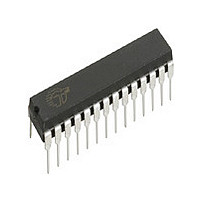
Package Type
PDIP
Operating Temperature Classification
Commercial
Operating Supply Voltage (max)
5.5V
Operating Supply Voltage (min)
4.5V
Operating Temp Range
0C to 70C
Pin Count
28
Mounting
Through Hole
Supply Current
70mA
Lead Free Status / Rohs Status
Compliant


Pin Configurations
Table 1. Pin Definitions - 28-Pin SOIC
Document Number: 001-50593 Rev. *A
Pin Name
DQ
A
0
V
V
WE
OE
CE
0
–A
SS
CC
-DQ
14
7
Alt
W
G
E
Power Supply Power Supply Inputs to the Device.
I/O Type
Input or
Ground
Output
Input
Input
Input
Input
Address Inputs. Used to select one of the 32,768 bytes of the nvSRAM.
Bidirectional Data I/O lines. Used as input or output lines depending on operation.
Write Enable Input, Active LOW. When the chip is enabled and WE is LOW, data on the
I/O pins is written to the specific address location.
Chip Enable Input, Active LOW. When LOW, selects the chip. When HIGH, deselects the
chip.
Output Enable, Active LOW. The active LOW OE input enables the data output buffers
during read cycles. Deasserting OE HIGH causes the I/O pins to tristate.
Ground for the Device. The device is connected to ground of the system.
Figure 1. Pin Diagram - 28-Pin SOIC
Description
STK15C88
Page 3 of 16
[+] Feedback
Related parts for STK15C88-WF45
Image
Part Number
Description
Manufacturer
Datasheet
Request
R

Part Number:
Description:
Manufacturer:
Cypress Semiconductor Corp
Datasheet:
Part Number:
Description:
STK15C88-NF25
Manufacturer:
Cypress Semiconductor Corp
Datasheet:
Part Number:
Description:
STK15C88-NF25I
Manufacturer:
Cypress Semiconductor Corp
Datasheet:
Part Number:
Description:
STK15C88-NF25ITR
Manufacturer:
Cypress Semiconductor Corp
Datasheet:
Part Number:
Description:
STK15C88-NF25TR
Manufacturer:
Cypress Semiconductor Corp
Datasheet:
Part Number:
Description:
STK15C88-NF45
Manufacturer:
Cypress Semiconductor Corp
Datasheet:
Part Number:
Description:
STK15C88-NF45I
Manufacturer:
Cypress Semiconductor Corp
Datasheet:
Part Number:
Description:
STK15C88-NF45ITR
Manufacturer:
Cypress Semiconductor Corp
Datasheet:
Part Number:
Description:
STK15C88-NF45TR
Manufacturer:
Cypress Semiconductor Corp
Datasheet:

Part Number:
Description:
STK15C88-SF25
Manufacturer:
Cypress Semiconductor Corp
Datasheet:
Part Number:
Description:
STK15C88-SF25I
Manufacturer:
Cypress Semiconductor Corp
Datasheet:
Part Number:
Description:
STK15C88-SF25ITR
Manufacturer:
Cypress Semiconductor Corp
Datasheet:
Part Number:
Description:
STK15C88-SF25TR
Manufacturer:
Cypress Semiconductor Corp
Datasheet:
Part Number:
Description:
STK15C88-SF45
Manufacturer:
Cypress Semiconductor Corp
Datasheet:
Part Number:
Description:
STK15C88-SF45I
Manufacturer:
Cypress Semiconductor Corp
Datasheet: