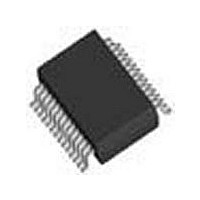
DS92LV1210TMSAX/NOPB National Semiconductor, DS92LV1210TMSAX/NOPB Datasheet - Page 4

DS92LV1210TMSAX/NOPB
Manufacturer Part Number
DS92LV1210TMSAX/NOPB
Description
Manufacturer
National Semiconductor
Datasheet
1.DS92LV1210TMSAXNOPB.pdf
(18 pages)
Specifications of DS92LV1210TMSAX/NOPB
Number Of Elements
1
Number Of Receivers
1
Number Of Drivers
10
Input Type
CMOS/TTL
Operating Supply Voltage (typ)
3.3V
Differential Input High Threshold Voltage
100mV
Diff. Input Low Threshold Volt
-100mV
Output Type
Deserializer
Transmission Data Rate
400Mbps
Power Dissipation
1.27W
Operating Temp Range
-40C to 85C
Operating Temperature Classification
Industrial
Mounting
Surface Mount
Pin Count
28
Package Type
SSOP-EIAJ
Lead Free Status / Rohs Status
Compliant
www.national.com
SERIALIZER CMOS/TTL DC SPECIFICATIONS (apply to DIN0-9, TCLK, PWRDN, TCLK_R/F, SYNC1, SYNC2, DEN)
V
V
V
I
DESERIALIZER CMOS/TTL DC SPECIFICATIONS (apply to pins PWRDN, RCLK_R/ F, REN, REFCLK = inputs; apply to
pins ROUT, RCLK, LOCK = outputs)
V
V
V
I
V
V
I
I
SERIALIZER Bus LVDS DC SPECIFICATIONS (apply to pins DO+ and DO−)
V
∆V
V
∆V
I
I
I
DESERIALIZER Bus LVDS DC SPECIFICATIONS (apply to pins RI+ and RI−)
VTH
VTL
IN
IN
OS
OZ
OS
OZ
OX
IH
IL
CL
IH
IL
CL
OH
OL
OD
OS
Absolute Maximum Ratings
If Military/Aerospace specified devices are required,
please contact the National Semiconductor Sales Office/
Distributors for availability and specifications.
Electrical Characteristics
Over recommended operating supply and temperature ranges unless otherwise specified.
Symbol
OD
OS
Supply Voltage (V
CMOS/TTL Input Voltage
CMOS/TTL Output
Voltage
Bus LVDS Receiver Input
Voltage
Bus LVDS Driver Output
Voltage
Bus LVDS Output Short
Circuit
Junction Temperature
Storage Temperature
Lead Temperature
Maximum Package Power Dissipation Capacity
(Soldering, 4 seconds)
High Level Input Voltage
Low Level Input Voltage
Input Clamp Voltage
Input Current
High Level Input Voltage
Low Level Input Voltage
Input Clamp Voltage
Input Current
High Level Output Voltage
Low Level Output Voltage
Output Short Circuit Current
TRI-STATE Output Current
Output Differential Voltage
(DO+)–(DO−)
Output Differential Voltage
Unbalance
Offset Voltage
Offset Voltage Unbalance
Output Short Circuit Current
TRI-STATE Output Current
Power-Off Output Current
Differential Threshold High Voltage
Differential Threshold Low Voltage
Duration
CC
Parameter
)
−0.3V to (V
−0.3V to (V
−65˚C to +150˚C
−0.3V to +3.9V
−0.3V to +3.9V
−0.3V to +4V
Continuous
CC
CC
+150˚C
+260˚C
+0.3V)
+0.3V)
(Note 1)
I
V
I
V
I
I
VOUT = 0V
PWRDN or REN = 0.8V, V
RL = 27Ω
D0 = 0V, DIN = High,PWRDN and DEN =
2.4V
PWRDN or DEN = 0.8V, DO = 0V or VCC
VCC = 0V, DO = 0V or VCC
VCM = +1.1V
CL
CL
OH
OL
IN
IN
= −18 mA
= −18 mA
= 9 mA
= 0V or 3.6V
= 0V or 3.6V
= −9 mA
4
Recommended Operating
Conditions
Conditions
Supply Voltage (V
Operating Free Air
Receiver Input Range
Supply Noise Voltage
Temperature (T
(V
@
Package Derating:
28L SSOP
ESD Rating (HBM)
CC
28L SSOP
25˚C Package:
)
OUT
= 0V or VCC
A
CC
)
)
200
Min
GND
GND
GND
−100
−40
0.78
3.0
Min
−10
−10
−15
−10
−10
−20
2.0
2.0
2.1
0
10.2 mW/˚C above
Nom
+25
−0.62
3.3
2.93
0.33
±
Typ
−38
270
−10
+19
1.1
±
±
±
±
−7
0.4
2
1
1
1
Max
+85
3.6
2.4
+100
1.27 W
Max
−1.5
−1.5
V
V
V
+10
+10
−85
+10
−15
+10
+20
100 mV
0.8
0.8
0.6
1.3
+25˚C
35
35
>
CC
CC
CC
5kV
Units
˚C
mV
V
V
Units
P-P
mA
mV
mV
mA
mV
mV
µA
µA
µA
µA
µA
V
V
V
V
V
V
V
V
V


