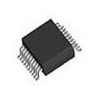
PI49FCT3807DH Pericom Semiconductor, PI49FCT3807DH Datasheet - Page 2

PI49FCT3807DH
Manufacturer Part Number
PI49FCT3807DH
Description
Manufacturer
Pericom Semiconductor
Datasheet
1.PI49FCT3807DH.pdf
(7 pages)
Specifications of PI49FCT3807DH
Number Of Outputs
10
Operating Supply Voltage (max)
3.6V
Operating Temp Range
-40C to 105C
Propagation Delay Time
3ns
Operating Supply Voltage (min)
3V
Mounting
Surface Mount
Pin Count
20
Operating Supply Voltage (typ)
3.3V
Package Type
SSOP
Quiescent Current
100nA
Input Frequency
156MHz
Operating Temperature Classification
Industrial
Dc
03+
Lead Free Status / Rohs Status
Not Compliant
Available stocks
Company
Part Number
Manufacturer
Quantity
Price
Company:
Part Number:
PI49FCT3807DHE
Manufacturer:
PERICOM
Quantity:
21
Part Number:
PI49FCT3807DHE
Manufacturer:
PERICOM
Quantity:
20 000
Company:
Part Number:
PI49FCT3807DHEX
Manufacturer:
PERICOM
Quantity:
446
Part Number:
PI49FCT3807DHEX
Manufacturer:
PERICOM
Quantity:
20 000
Maximum Ratings
(Above which the useful life may be impaired. For user guidelines, not tested.)
Operating Range
DC Electrical Characteristics
Notes:
1. For Max. or Min. conditions, use appropriate value specifi ed under Electrical Characteristics for the applicable device type.
2. Typical values are at V
3. V
4. This parameter is determined by device characterization but is not production tested.
5. Not more than one output should be shorted at one time. Duration of the test should not exceed one second.
Parameters Description
V
Industrial Temperature ......................................................–40°C to +105°C
Input Frequency.................................................................... DC to 156 MHz
Storage Temperature ...........................................................–65°C to +150°C
V
Output Voltage ............................................................... –0.5V to V
Input Voltage .........................................................................–0.5V to +5.5V
DD
DD
I
I
V
V
V
V
V
ODH
ODL
I
I
OH
Voltage ............................................................................... 3.3V ± 0.3V
IH
Voltage ..........................................................................–0.5V to +4.6V
IL
OH
OL
IH
IK
IL
08-0002
= V
DD
Input HIGH Voltage
Input LOW Voltage
Input HIGH Current
Input LOW Current
Clamp Diode Voltage
Output High Voltage
Output LOW Voltage
Output HIGH Current
Output LOW Current
– 0.6V at rated current.
DD
= 3.3V, +25°C ambient and maximum loading.
(Over the Operating Range)
Guaranteed Logic HIGH level (Input Pins)
Guaranteed Logic LOW level (Input Pins)
V
V
V
V
V
V
Test Conditions
V
DD
DD
DD
DD
DD
DD
DD
= Max
= Max
= Min. I
= Min. V
= 3.3V, V
= 3.3V, V
= Min. V
IN
IN
IN
IN
IN
= -18mA
(1)
= V
= V
= V
= V
IH
IH
IH
IH
2
DD
or V
or V
or V
or V
+0.5V
IL
IL
IL
IL
1-10 Clock Buffer for Networking Applications
, V
, V
OUT
OUT
V
V
I
I
I
I
OH
OH
OL
OL
IN
IN
Note:
Stresses greater than those listed under MAXIMUM
RAT INGS may cause permanent damage to the
device. This is a stress rating only and functional op er a tion
of the device at these or any other con di tions above those
indicated in the operational sec tions of this spec i fi ca tion is
not implied. Ex po sure to absolute maximum rating con di -
tions for extended periods may affect re li abil i ty.
= 1.5V
= 1.5V
= 0.1mA
= 12mA
= 0.1mA
= -12mA
= 5.5V
= GND
(4, 5)
(4, 5)
Min.
V
2.4
DD
-0.5
-45
2.0
50
-0.2
(3)
Typ.
-0.7
-75
3.0
0.3
80
(2)
PI49FCT3807D
Max.
PS8493D
-180
-1.2
200
5.5
0.8
0.2
0.5
1
1
Units
mA
01/08/08
μA
V
V


