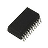
PI5C3401SX Pericom Semiconductor, PI5C3401SX Datasheet - Page 2

PI5C3401SX
Manufacturer Part Number
PI5C3401SX
Description
Manufacturer
Pericom Semiconductor
Datasheet
1.PI5C3401SX.pdf
(5 pages)
Specifications of PI5C3401SX
Function
Bus Exchange Switch
Operating Temperature (max)
85C
Operating Temperature (min)
-40C
Package Type
SOIC
Pin Count
24
Mounting
Surface Mount
Lead Free Status / Rohs Status
Not Compliant
DC Electrical Characteristics
Notes:
1.
2.
3.
4.
Capacitance
Notes:
1.
Parameters
Maximum Ratings
(Above which the useful life may be impaired. For user guidelines, not tested.)
Storage Temperature ..........................................................–65°C to +150°C
Ambient Temperature with Power Applied .........................–40°C to +85°C
Supply Voltage to Ground Potential .....................................–0.5V to +7.0V
DC Input Voltage ..................................................................–0.5V to +7.0V
DC Output Current ............................................................................120 mA
Power Dissipation .................................................................................0.5W
Parameters
For Max. or Min. conditions, use appropriate value specifi ed under Electrical Characteristics for the applicable device type.
Typical values are at Vcc = 5.0V, T
Not more than one output should be shorted at one time. Duration of the test should not exceed one second.
Measured by the voltage drop between A and B pin at indicated current through the switch. ON resistance is determined by the lower of the
voltages on the two (A,B) pins.
This parameter is determined by device characterization but is not production tested.
R
V
V
V
I
I
V
I
I
OZ
OS
IH
ON
IL
IH
IK
IL
H
07-0127
C
C
C
OFF
ON
IN
Input HIGH Voltage
Input LOW Voltage
Input HIGH Current
Input LOW Current
High Impedance Output Current
Clamp Diode Voltage
Short Circuit Current
Input Hysteresis at Control Pins
Switch On-Resistance
(1)
(T
A
= 25°C, f = 1 MHz)
Input Capacitance
A/B Capacitance, Switch Off
A/B Capacitance, Switch On
De scrip tion
De scrip tion
A
(3)
= 25°C ambient and maximum loading.
(4)
(Over the Operating Range, T
Guaranteed Logic HIGH Level
Guaranteed Logic LOW Level
V
V
0 ≤ A, B ≤ V
V
A (B) = 0V, B (A) = V
V
V
CC
CC
CC
CC
CC
= Max., V
= Max., V
= Min., I
= Min., V
= Min., V
Test Conditions
V
Test Conditions
IN
CC
2
IN
IN
IN
A
= 0V
IN
IN
= –18 mA
= –40°C to +85°C, V
= 0.0V, I
= 2.4V, I
= V
= GND
CC
CC
ON
ON
Note:
Stresses greater than those listed under MAXIMUM RAT-
INGS may cause permanent damage to the device. This is a
stress rating only and functional operation of the device at
these or any other con di tions above those indicated in the
operational sections of this spec i fi ca tion is not implied. Ex-
posure to absolute maximum rating conditions for extended
periods may affect re li abil i ty.
(1)
= 48mA
= 15mA
Typ.
6-Bit, 3-Port Bus Exchange Switch
CC
= 5V ±5%)
Min.
–0.5
100
2.0
Max.
6
6
8
Typ
–0.7
150
10
5
(2)
PS7020E
Max.
–1.2
0.8
±1
±1
±1
15
7
PI5C3401
Units
pF
Units
mV
mA
μA
Ω
05/02/07
V
V


