IDTV386GLFT IDT, Integrated Device Technology Inc, IDTV386GLFT Datasheet
IDTV386GLFT
Specifications of IDTV386GLFT


Related parts for IDTV386GLFT


IDTV386GLFT Summary of contents
Page 1
V386 8-B LVDS R IT General Description The V386 is an ideal LVDS receiver that converts 4-pair LVDS data streams into parallel 28 bits of CMOS/TTL data with bandwidth up to 2.38 Gbps throughput or 297.5 Mbytes per second. This ...
Page 2
V386 8-B LVDS R IT ECEIVER FOR Pin Descriptions Pin Pin name Type 1 RxOUT22 OUT 2 RxOUT23 OUT 3 RxOUT24 OUT 4 GND Ground 5 RxOUT25 OUT 6 RxOUT26 OUT 7 RxOUT27 OUT 8 LVDS_GND Ground 9 RxIN0- LVDS ...
Page 3
V386 8-B LVDS R IT ECEIVER FOR Pin Pin name Type 34 RxOUT5 OUT 35 RxOUT6 OUT 36 GND Ground 37 RxOUT7 OUT 38 RxOUT8 OUT 39 RxOUT9 OUT 40 VCC Power 41 RxOUT10 OUT 42 RxOUT11 OUT 43 RxOUT12 ...
Page 4
V386 8-B LVDS R IT ECEIVER FOR Absolute Maximum Ratings Stresses above the ratings listed below can cause permanent damage to the V386. These ratings, which are standard values for ICS commercially rated parts, are stress ratings only. Functional operation ...
Page 5
V386 8-B LVDS R IT ECEIVER FOR Parameter Output Short Circuit Current LVDS Receiver DC Specifications Differential Input High Threshold Differential Input Low Threshold Input Current Receiver Supply Current Receiver Supply Current (worst case) Receiver Supply Current (16 Grayscale) Receiver ...
Page 6
V386 8-B LVDS R IT ECEIVER FOR Parameter Receiver Input Strobe Position for Bit5 Receiver Input Strobe Position for Bit6 RxIn Skew Margin (see note and Figure 8) Note: The skew margins mean the maximum timing tolerance between the clock ...
Page 7
V386 8-B LVDS R IT ECEIVER FOR Timing Diagrams CLKIN/CLKOUT ODD Data In/Data Out EVEN Data In/Data Out Figure 1a. “Worst Case” Test Pattern CLKOUT D0 D1 D2, 10, 18 D3, 11, 19 D4-7, 12-15, 20-23 ...
Page 8
V386 8-B LVDS R IT ECEIVER FOR 0.8 V CLKOUT D0 – D27 Out Figure 3. V386 SETUP/HOLD and High/Low Times RCK CLKOUT Figure 4. V386 Clock In to Clock Out Delay 2.0 V PWRDWN 3.0 V VCC RCK CLKOUT ...
Page 9
V386 8-B LVDS R IT ECEIVER FOR Clock Previous Cycle Data Rspos0 Min Rspos0 Max Rspos1 Min Rspos1 Max Rspos2 Min Rspos2 Max Figure 7. V386 LVDS Input Strobe Position RCK+/RCK- RX[n]+/RX[n Figure 8. ...
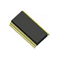
Page 10
V386 8-B LVDS R IT ECEIVER FOR Package Outline and Package Dimensions Package dimensions are kept current with JEDEC Publication No INDEX AREA Ordering Information Part / Order Number Marking V386GLF ...