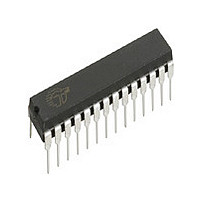
STK20C04-W25 Cypress Semiconductor Corp, STK20C04-W25 Datasheet - Page 3

STK20C04-W25
Manufacturer Part Number
STK20C04-W25
Description
Manufacturer
Cypress Semiconductor Corp
Type
NVSRAMr
Datasheet
1.STK20C04-W25.pdf
(12 pages)
Specifications of STK20C04-W25
Word Size
8b
Organization
512x8
Density
4Kb
Interface Type
Parallel
Access Time (max)
25ns
Operating Supply Voltage (typ)
5V
Package Type
PDIP
Operating Temperature Classification
Commercial
Operating Supply Voltage (max)
5.5V
Operating Supply Voltage (min)
4.5V
Operating Temp Range
0C to 70C
Pin Count
28
Mounting
Through Hole
Supply Current
85mA
Lead Free Status / Rohs Status
Compliant
March 2006
SRAM READ CYCLES #1 & #2
Note f:
Note g: I/O state assumes E, G < V
Note h: Measured + 200mV from steady state output voltage.
SRAM READ CYCLE #1: Address Controlled
SRAM READ CYCLE #2: E Controlled
DQ (DATA OUT)
DQ (DATA OUT)
NO.
10
11
1
2
3
4
5
6
7
8
9
ADDRESS
ADDRESS
W must be high during SRAM READ cycles and low during SRAM WRITE cycles. NE must be high during entire cycle.
t
t
t
t
t
t
t
t
t
t
t
ELQV
AVAV
AVQV
GLQV
AXQX
ELQX
EHQZ
GLQX
GHQZ
ELICCH
EHICCL
#1, #2
I
CC
G
E
f
g
g
h
h
SYMBOLS
e
d, e
t
t
t
t
t
t
t
t
t
t
t
ACS
RC
AA
OE
OH
LZ
HZ
OLZ
OHZ
PA
PS
Alt.
IL
, W > V
STANDBY
Chip Enable Access Time
Read Cycle Time
Address Access Time
Output Enable to Data Valid
Output Hold after Address Change
Chip Enable to Output Active
Chip Disable to Output Inactive
Output Enable to Output Active
Output Disable to Output Inactive
Chip Enable to Power Active
Chip Disable to Power Standby
t
IH
ELICCH
t
ELQX
, and NE ≥ V
t
AXQX
10
t
6
GLQX
5
8
t
GLQV
PARAMETER
4
IH
; device is continuously selected.
t
AVAV
f
t
ELQV
2
ACTIVE
t
AVQV
1
3
t
AVAV
3
2
f, g
Document Control # ML0001 rev 0.2
DATA VALID
STK20C04-25
MIN
25
5
5
0
0
MAX
25
25
10
10
10
25
DATA VALID
STK20C04-35
MIN
35
5
5
0
0
(V
t
GHQZ
9
t
CC
EHQZ
MAX
35
35
15
13
13
35
7
t
EHICCL
= 5.0V
11
STK20C04-45
MIN
STK20C04
45
5
5
0
0
MAX
45
45
20
15
15
45
±
10%)
UNITS
ns
ns
ns
ns
ns
ns
ns
ns
ns
ns
ns


