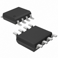
MAX522CSA Maxim Integrated Products, MAX522CSA Datasheet - Page 7

MAX522CSA
Manufacturer Part Number
MAX522CSA
Description
IC DAC DUAL V-OUT SRL 8BIT 8SOIC
Manufacturer
Maxim Integrated Products
Datasheet
1.MAX522CPA.pdf
(12 pages)
Specifications of MAX522CSA
Settling Time
70µs
Number Of Bits
8
Data Interface
Serial
Number Of Converters
2
Voltage Supply Source
Single Supply
Operating Temperature
0°C ~ 70°C
Mounting Type
Surface Mount
Package / Case
8-SOIC (3.9mm Width)
Lead Free Status / RoHS Status
Contains lead / RoHS non-compliant
Power Dissipation (max)
-
Available stocks
Company
Part Number
Manufacturer
Quantity
Price
Company:
Part Number:
MAX522CSA
Manufacturer:
MAXIM
Quantity:
14
Part Number:
MAX522CSA
Manufacturer:
MAXIM/美信
Quantity:
20 000
Company:
Part Number:
MAX522CSA+T
Manufacturer:
MAXIM
Quantity:
2 292
Company:
Part Number:
MAX522CSA+T
Manufacturer:
THAILAND
Quantity:
6 237
Part Number:
MAX522CSA+T
Manufacturer:
MAXIM/美信
Quantity:
20 000
The MAX522 contains two 8-bit, voltage-output digital-
to-analog converters (DACs). The DACs are “inverted”
R-2R ladder networks using complementary switches
that convert 8-bit digital inputs into equivalent analog
output voltages in proportion to the applied reference
voltage.
The MAX522 has one reference input which is shared
by DAC A and DAC B. The device includes output
buffer amplifiers for both DACs and input logic for sim-
ple microprocessor (µP) and CMOS interfaces. The
power-supply range is from +5.5V down to +2.7V.
The voltage at REF sets the full-scale output of the
DACs. The input impedance of the REF input is code
dependent. The lowest value, approximately 8kΩ,
occurs when the input code is 01010101 (55hex). The
maximum value of infinity occurs when the input code
is zero.
In shutdown mode, the selected DAC output is set to
zero while the value stored in the DAC register remains
unchanged. This removes the load from the reference
input to save power. Bringing the MAX522 out of shut-
down mode restores the DAC output voltage. Because
the input resistance at REF is code dependent, the
DAC’s reference sources should have an output
impedance of no more than 5Ω. The input capacitance
at the REF pin is also code dependent and typically
does not exceed 25pF.
______________________________________________________________Pin Description
_______________Detailed Description
PIN
1
2
3
4
5
6
7
8
NAME
OUTA
OUTB
SCLK
GND
V
REF
DIN
–
C
Reference Input and DAC Output Range
—
DD
S
–
_______________________________________________________________________________________
Chip Select (active low). Enables data to be shifted into the 16-bit shift register. Programming commands
are executed at the rising edge of
Serial Clock Input. Data is clocked in on the rising edge of SCLK.
Positive Power Supply (2.7V to 5.5V). Bypass with 0.22µF to GND.
Ground
DAC A Output Voltage (Buffered). Connect 0.1µF capacitor or greater to GND.
DAC B Output Voltage (Buffered). Connect 0.01µF capacitor or greater to GND.
Reference Input for DAC A and DAC B
Serial Data Input of the 16-bit shift register. Data is clocked into the register on the rising edge of SCLK.
Analog Section
Serial DAC in 8-Pin SO Package
Dual, 8-Bit, Voltage-Output
–
C
—
S
–
.
The reference voltage on REF can range anywhere from
GND to V
more information.
DAC A and DAC B voltage outputs are internally
buffered. The buffer amplifiers have a rail-to-rail
(GND to V
The DAC outputs are internally divided by two and the
buffer is set to a gain of two, eliminating the need for a
buffer input voltage range to the positive supply rail.
DAC A’s output amplifier can source and sink up to
5mA of current (0.5mA for DAC B’s buffer). See the
Total Unadjusted Error vs. Digital Code graph in the
Typical Operating Characteristics . The amplifier is
unity-gain stable with a capacitive load of 0.1µF
(0.01µF for DAC B’s buffer) or greater. The slew rate is
limited by the load capacitor and is typically 0.1V/µs
with a 0.1µF load (0.01µF for DAC B’s buffer).
When programmed to shutdown mode, the outputs of
DAC A and DAC B go into a high-impedance state.
Virtually no current flows into or out of the buffer ampli-
fiers in that state. In shutdown mode, the REF inputs
are high impedance (2MΩ typical) to conserve current
drain from the system reference; therefore, the system
reference does not have to be powered down.
Coming out of shutdown, the DAC outputs return to the
values kept in the registers. The recovery time is equiv-
alent to the DAC settling time.
FUNCTION
DD
DD
. See the Output Buffer Amplifier section for
) output voltage range.
Output Buffer Amplifiers
Shutdown Mode
7


