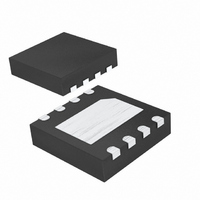
MAX5547ETA+T Maxim Integrated Products, MAX5547ETA+T Datasheet - Page 2

MAX5547ETA+T
Manufacturer Part Number
MAX5547ETA+T
Description
IC DAC 10BIT DUAL 8-TDFN
Manufacturer
Maxim Integrated Products
Datasheet
1.MAX5547ETAT.pdf
(12 pages)
Specifications of MAX5547ETA+T
Settling Time
10µs
Number Of Bits
10
Data Interface
Serial
Number Of Converters
2
Voltage Supply Source
Single Supply
Operating Temperature
-40°C ~ 85°C
Mounting Type
Surface Mount
Package / Case
8-TDFN Exposed Pad
Lead Free Status / RoHS Status
Lead free / RoHS Compliant
Power Dissipation (max)
-
ABSOLUTE MAXIMUM RATINGS
V
OUTA, OUTB, REF to GND ........................-0.3V to (V
SCLK, DIN, CS to GND ............................................-0.3V to +6V
Continuous Power Dissipation (T
Dual, 10-Bit, Current-Sink Output DAC
ELECTRICAL CHARACTERISTICS
(V
V
Stresses beyond those listed under “Absolute Maximum Ratings” may cause permanent damage to the device. These are stress ratings only, and functional
operation of the device at these or any other conditions beyond those indicated in the operational sections of the specifications is not implied. Exposure to
absolute maximum rating conditions for extended periods may affect device reliability.
2
STATIC PERFORMANCE—ANALOG SECTION
Resolution
Integral Nonlinearity (Note 2)
Differential Nonlinearity
Offset Error
Offset Temperature Coefficent
Gain Error
Gain Temperature Coefficient
Line Regulation
Output Crosstalk
REFERENCE
Internal-Reference Voltage
Internal-Reference Temperature
Coefficient
Internal-Reference Load
Regulation
Internal-Reference Power-Up
Time
Internal-Reference Sink Current
Internal-Reference Source
Current
REF Capacitive Load
Reference Line Regulation
Internal-Reference Noise
External-Reference Range
DD
DD
8-Pin TDFN (derate 18.2mW/°C above +70°C) .......1454.5mW
DD
_______________________________________________________________________________________
to GND .............................................................-0.3V to +6V
= +3.0V, and T
= +2.7V to +5.25V, V
PARAMETER
A
= +25°C.) (Note 1)
GND
= 0V, external reference = +2.5V, output voltage = +2.0V, T
A
= +70°C)
SYMBOL
V
V
DNL
INL
OE
GE
REF
REF
I
I
Guaranteed monotonic
Code = 030h, T
(Note 3)
Measured from code
030h to 3FFh
I
I
V
OUTA = midscale, OUTB switching from
030h to 3FFh
T
(Note 4)
0µA < I
C
(Note 4)
V
f = 0.1Hz to 10Hz
f = 10Hz to 10kHz
OUT
OUT
OUT_
OUT_
A
DD
DD
REF
DD
= +25°C
_ = 1.2mA
_ = 3.6mA
= +2.7V to +5.25V
= +2.7V to +5.25V
= 1µF, to 0.05%
+ 0.3V)
= 1.2mA
= 3.6mA
REF
< +300µA
CONDITIONS
A
= +25°C
Operating Temperature Range ...........................-40°C to +85°C
Junction Temperature .....................................................+150°C
Storage Temperature Range ............................-65°C to +150°C
Lead Temperature (soldering, 10s) ................................+300°C
I
I
OUT
OUT
_ = 1.2mA
_ = 3.6mA
A
= -40°C to +85°C. Typical values are at
2.48
2.45
MIN
0.1
10
±0.1
±0.1
0.55
TYP
0.05
2.5
±1
±1
25
10
27
15
25
54
4
1
±0.75
MAX
±5.5
0.15
2.52
10.0
2.55
300
0.8
3.5
±6
±6
±9
±3
30
50
ppm/°C
ppm/°C
LSB/°C
UNITS
µV
LSB/V
µV/V
LSB
LSB
LSB
Bits
ms
dB
µA
µA
µF
%
Ω
V
RMS
V


