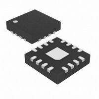
MAX5548ETE+ Maxim Integrated Products, MAX5548ETE+ Datasheet - Page 2

MAX5548ETE+
Manufacturer Part Number
MAX5548ETE+
Description
IC DAC 8BIT DUAL 30MA 16-TQFN
Manufacturer
Maxim Integrated Products
Datasheet
1.MAX5548ETE.pdf
(15 pages)
Specifications of MAX5548ETE+
Settling Time
30µs
Number Of Bits
8
Data Interface
Serial
Number Of Converters
2
Voltage Supply Source
Single Supply
Operating Temperature
-40°C ~ 85°C
Mounting Type
Surface Mount
Package / Case
16-TQFN Exposed Pad
Lead Free Status / RoHS Status
Lead free / RoHS Compliant
Power Dissipation (max)
-
ABSOLUTE MAXIMUM RATINGS
V
OUTA, OUTB to GND .................................-0.3V to (V
REFIN CS/AO, DOUT/AI, SPI/I2C, FSADJA,
SCLK/SCL, DIN/SDA ................................................-0.3V to +6V
Continuous Power Dissipation (T
Dual, 8-Bit, Programmable, 30mA
High-Output-Current DAC
Stresses beyond those listed under “Absolute Maximum Ratings” may cause permanent damage to the device. These are stress ratings only, and functional
operation of the device at these or any other conditions beyond those indicated in the operational sections of the specifications is not implied. Exposure to
absolute maximum rating conditions for extended periods may affect device reliability.
ELECTRICAL CHARACTERISTICS
(V
V
2
STATIC PERFORMANCE—ANALOG SECTION
Resolution
Integral Nonlinearity
Differential Nonlinearity
Offset
Zero-Scale Error
Full-Scale Error
REFERENCE
Internal Reference Range
Internal Reference Tempco
External Reference Range
External Reference Input Current
DAC OUTPUTS
Full-Scale Current
Output Current Leakage in
Shutdown
Output Capacitance
Current Source Dropout Voltage
(V
Output Impedance at Full-Scale
Current
Capacitive Load to Ground
Series Inductive Load
Maximum FSADJ_ Capacitive
Load
DYNAMIC PERFORMANCE
Settling Time
Digital Feedthrough
Digital-to-Analog Glitch Impulse
DD
SCLK/SCL
16-Pin Thin QFN (derate 17.5mW/°C above +70°C) ..1398.6mW
FSADJB to GND ......................................-0.3V to (V
DD
DD
_______________________________________________________________________________________
to GND .............................................................-0.3V to +6V
= +2.7V to +5.25V, GND = 0, V
- V
OUT
PARAMETER
= 0, T
_)
A
= -40°C to +85°C, unless otherwise noted. Typical values are at V
A
= +85°C)
SYMBOL
C
C
L
FSADJ_
REFIN
DNL
LOAD
INL
LOAD
I
OS
t
S
= +1.25V, internal reference, R
I
Guaranteed monotonic
I
I
includes offset
(Note 3)
I
I
C
OUT
OUT
OUT
OUT
OUT
LOAD
DD
DD
_ = 1mA to 30mA (Note 2)
_ = 1mA to 30mA, code = 0x00
_ = 1mA to 30mA, code = 0xFF,
_ = 30mA
_ = 20mA
+ 0.3V)
+ 0.3V)
= 24pF, L
CONDITIONS
LOAD
Operating Temperature Range ...........................-40°C to +85°C
Junction Temperature .....................................................+150°C
Storage Temperature Range ............................-65°C to +150°C
Lead Temperature (soldering, 10s) ................................+300°C
= 27nH (Note 4)
T
T
A
A
= +25°C
= -40°C to +85°C
FSADJ_
DD
= 20kΩ; compliance voltage = (V
= +3.0V and T
MIN
1.21
0.55
-13
0.5
0.6
8
1
1
A
= +25°C.) (Note 1)
TYP
1.25
108
100
100
±1
30
10
10
75
30
40
-4
-4
2
MAX
1.29
225
1.5
±1
±1
30
1
DD
ppm/°C
UNITS
- 0.6V),
LSB
LSB
LSB
LSB
Bits
nVs
nVs
mA
µA
µA
µA
pF
kΩ
nH
pF
nF
µs
V
V
V


