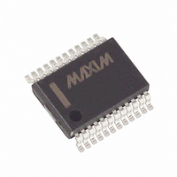
MAX521BCAG Maxim Integrated Products, MAX521BCAG Datasheet - Page 9

MAX521BCAG
Manufacturer Part Number
MAX521BCAG
Description
IC DAC OCTAL SER 8BIT R/R 24SSOP
Manufacturer
Maxim Integrated Products
Datasheet
1.MAX520BCPE.pdf
(20 pages)
Specifications of MAX521BCAG
Settling Time
6µs
Number Of Bits
8
Data Interface
I²C, Serial
Number Of Converters
8
Voltage Supply Source
Single Supply
Power Dissipation (max)
640mW
Operating Temperature
0°C ~ 70°C
Mounting Type
Surface Mount
Package / Case
24-SSOP
Lead Free Status / RoHS Status
Contains lead / RoHS non-compliant
Figure 1. 2-Wire Serial-Interface Timing Diagram
______________________________________________________________Pin Description
SDA
SCL
DIP/SO
10
11
12
13
14
15
16
—
—
—
—
—
—
1
2
3
4
6
5
7
8
9
t
HD
START CONDITION
,
STA
MAX520
4, 7, 14, 17
_______________________________________________________________________________________
SSOP
10
—
—
—
—
11
12
13
15
—
16
18
19
20
1
2
3
5
8
6
9
t
LOW
t
R
Quad/Octal, 2-Wire Serial 8-Bit DACs
t
PIN
SU
t
HIGH
,
DAT
t
F
DIP
10
11
12
13
14
15
16
17
18
19
20
—
—
1
2
3
4
5
6
7
8
9
t
HD
,
MAX521
DAT
7, 9, 16, 20
SO/SSOP
10
11
12
13
14
15
17
18
19
21
22
23
24
—
1
2
3
4
5
6
8
t
SU
REPEATED START CONDITION
,
STA
with Rail-to-Rail Outputs
NAME
DGND
AGND
OUT1
OUT0
OUT4
OUT5
OUT6
OUT7
OUT3
OUT2
REF1
REF0
REF4
REF3
REF2
N.C.
SCL
SDA
AD0
AD1
AD2
V
DD
t
HD
,
STA
DAC1 Voltage Output
DAC0 Voltage Output
Reference Voltage Input for DAC1
Reference Voltage Input for DAC0
No Connect—not internally connected
Digital Ground
Analog Ground
Serial Clock Input
Serial Data Input
DAC4 Voltage Output
DAC5 Voltage Output
DAC6 Voltage Output
DAC7 Voltage Output
Address Input 0; sets IC’s slave address
Address Input 1; sets IC’s slave address
Address Input 2; sets IC’s slave address
Power Supply, +5V
Reference Voltage Input for DACs 4, 5, 6, and 7
Reference Voltage Input for DAC3
Reference Voltage Input for DAC2
DAC3 Voltage Output
DAC2 Voltage Output
t
SU
,
STO
FUNCTION
STOP CONDITION
t
BUF
START CONDITION
9


