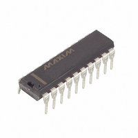
MAX5250BCPP Maxim Integrated Products, MAX5250BCPP Datasheet - Page 2

MAX5250BCPP
Manufacturer Part Number
MAX5250BCPP
Description
IC DAC QUAD V-OUT 10BIT LP 20DIP
Manufacturer
Maxim Integrated Products
Datasheet
1.MAX5250BCPP.pdf
(16 pages)
Specifications of MAX5250BCPP
Settling Time
10µs
Number Of Bits
10
Data Interface
Serial
Number Of Converters
4
Voltage Supply Source
Single Supply
Operating Temperature
0°C ~ 70°C
Mounting Type
Through Hole
Package / Case
20-DIP (0.300", 7.62mm)
Lead Free Status / RoHS Status
Contains lead / RoHS non-compliant
Power Dissipation (max)
-
Available stocks
Company
Part Number
Manufacturer
Quantity
Price
Company:
Part Number:
MAX5250BCPP+
Manufacturer:
Maxim Integrated Products
Quantity:
1 951
ABSOLUTE MAXIMUM RATINGS
V
V
AGND to DGND ..................................................................±0.3V
REFAB, REFCD to AGND ...........................-0.3V to (V
OUT_, FB_ to AGND...................................-0.3V to (V
Digital Inputs to DGND.............................................-0.3V to +6V
DOUT, UPO to DGND ................................-0.3V to (V
Continuous Current into Any Pin.......................................±20mA
ELECTRICAL CHARACTERISTICS
(V
noted. Typical values are at T
Low-Power, Quad, 10-Bit Voltage-Output DAC
with Serial Interface
Stresses beyond those listed under “Absolute Maximum Ratings” may cause permanent damage to the device. These are stress ratings only, and functional
operation of the device at these or any other conditions beyond those indicated in the operational sections of the specifications is not implied. Exposure to
absolute maximum rating conditions for extended periods may affect device reliability.
2
DD
DD
STATIC PERFORMANCE—ANALOG SECTION
REFERENCE INPUT
MULTIPLYING-MODE PERFORMANCE
Resolution
Integral Nonlinearity
(Note 1)
Differential Nonlinearity
Offset Error
Offset-Error Tempco
Gain Error
Gain-Error Tempco
Power-Supply Rejection Ratio
Reference Input Range
Reference Input Resistance
Reference -3dB Bandwidth
Reference Feedthrough
Signal-to-Noise Plus
Distortion Ratio
DD
_______________________________________________________________________________________
to AGND............................................................-0.3V to +6V
to DGND ...........................................................-0.3V to +6V
= +5V ±10%, AGND = DGND = 0V, REFAB = REFCD = 2.5V, R
PARAMETER
A
= +25°C. Output buffer connected in unity-gain configuration (Figure 9).)
SYMBOL
SINAD
PSRR
R
V
DNL
V
INL
GE
REF
REF
N
OS
MAX5250A
MAX5250B
Guaranteed monotonic
(Note 1)
4.5V ≤ V
Code dependent, minimum at code 554 hex
V
Input code = all 0s, V
V
REF
REF
DD
DD
DD
= 0.67V
= 1V
+ 0.3V)
+ 0.3V)
+ 0.3V)
DD
P-P
≤ 5.5V
P-P
at 25kHz, code = full scale
CONDITIONS
REF
Continuous Power Dissipation (T
Operating Temperature Ranges
Storage Temperature Range .............................-65°C to +150°C
Lead Temperature (soldering, 10s) .................................+300°C
Plastic DIP (derate 8.00mW/°C above +70°C) .................640mW
SSOP (derate 8.00mW/°C above +70°C) ......................640mW
CERDIP (derate 11.11mW/°C above +70°C) .................889mW
MAX5250_C_P ......................................................0°C to +70°C
MAX5250_E_P ...................................................-40°C to +85°C
MAX5250BMJP ................................................-55°C to +125°C
L
= 3.6V
= 5kΩ, C
P-P
L
at 1kHz
= 100pF, T
A
MIN
10
0
8
= T
A
MIN
= +70°C)
±0.25
TYP
to T
100
650
-84
72
6
1
MAX
V
DD
, unless otherwise
MAX
±0.5
±1.0
±1.0
±6.0
±1.0
800
- 1.4
ppm/°C
ppm/°C
UNITS
µV/V
LSB
LSB
LSB
Bits
kHz
mV
kΩ
dB
dB
V


