YM05S05 POWER ONE, YM05S05 Datasheet - Page 5
YM05S05
Manufacturer Part Number
YM05S05
Description
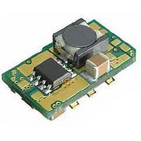
Module DC-DC 1-OUT 0.7525V to 3.63V 5A 5-Pin SMD
Manufacturer
POWER ONE
Type
Step Downr
Datasheet
1.YM05S05-G.pdf
(24 pages)
Specifications of YM05S05
Package
5SMD
Output Current
5 A
Output Voltage
0.7525 to 3.63 V
Input Voltage
5 V
Number Of Outputs
1
Product
Non-Isolated / POL
Input Voltage Range
4.5 V to 5.5 V
Input Voltage (nominal)
5 V
Output Current (channel 1)
5 A
Package / Case Size
DIP
Output Type
Regulated
Package / Case
DIP
Lead Free Status / Rohs Status
Lead free / RoHS Compliant
Available stocks
Company
Part Number
Manufacturer
Quantity
Price
Company:

Part Number:
YM05S05
Manufacturer:
PERICOM
Quantity:
201
Part Number:
YM05S05
Manufacturer:
POWER-ONE
Quantity:
20 000
Company:
Part Number:
YM05S05-G
Manufacturer:
BELPOWER
Quantity:
200
Part Number:
YM05S05-G
Manufacturer:
BEL
Quantity:
20 000


Operations
Input and Output Impedance
The Y-Series converter should be connected via a
low impedance to the DC power source. In many
applications, the inductance associated with the
distribution from the power source to the input of the
converter can affect the stability of the converter. It is
recommended to use decoupling capacitors in order
to ensure stability of the converter and reduce input
ripple voltage. Internally, the converter has 20
(low ESR ceramics) of input capacitance.
In a typical application, low - ESR tantalum or POS
capacitors will be sufficient to provide adequate
ripple voltage filtering at the input of the converter.
However,
47
converter in order to minimize the input ripple
voltage. They should be placed as close as possible
to the input pins of the converter.
The YM05S05 has been designed for stable
operation with or without external capacitance. Low
ESR ceramic capacitors placed as close as possible
to the load (minimum 47
improved transient performance and lower output
voltage ripple.
It is important to keep low resistance and low
inductance PCB traces for connecting your load to
the output pins of the converter. This is required to
maintain good load regulation since the converter
does not have a SENSE pin for compensating
voltage drops associated with the power distribution
system on your PCB.
ON/OFF (Pin 1)
The ON/OFF pin (Pin 1) is used to turn the converter
on or off remotely via a system signal that is
referenced to GND (Pin 4). Typical connections are
shown in Fig. A.
ZD-01978 Rev. 3.2, 18-Jun-10
Vin
Vin
CONTROL
-
INPUT
100
Fig. A: Circuit configuration for ON/OFF function.
µ
R*
F are recommended at the input of the
very
GND
ON/OFF
Vin
low
(Top View)
Converter
Y-Series
ESR
µ
F) are recommended for
3.0-5.5 VDC Input; 0.7525-3.63 VDC Programmable @ 5 A
ceramic
TRIM
Vout
capacitors
www.power-one.com
Rload
µ
F
To turn the converter on the ON/OFF pin should be
at a logic low or left open, and to turn the converter
off the ON/OFF pin should be at a logic high or
connected to Vin.
ON/OFF pin is internally pulled-down. A TTL or
CMOS logic gate, open collector (open drain)
transistor can be used to drive ON/OFF pin. When
using open collector (open drain) transistor, add a
pull-up resistor (R*) of 5 K to Vin as shown in Fig. A.
The external pull-up resistor can be increased to 10K
if the minimum input voltage is more than 3.0 V and
to 20K if the minimum voltage is more than 4.5 V.
This device must be capable of:
–
–
Output Voltage Programming (Pin 3)
The output voltage can be programmed from
0.7525 V to 3.63 V by connecting an external resistor
between TRIM pin (Pin 3) and GND pin (Pin 4); see
Fig. B. Note that when a trim resistor is not
connected, the output voltage of the converter is
0.7525 V.
A trim resistor, R
can be calculated using the following equation:
where,
Note that the tolerance of a trim resistor directly
affects
recommended to use standard 1% or 0.5% resistors;
for tighter tolerance, two resistors in parallel are
Vin
R
R
V
T
TRIM
O
Fig. B: Configuration for programming output voltage.
RIM
REQ
sinking up to 1.2 mA at a low level voltage of
0.8 V
sourcing up to 0.25 mA at a high logic level of
2.3 V – 5.5 V.
Required value of trim resistor [k]
(V
Desired (trimmed) output voltage [V]
the
O
YM05S05 DC-DC Converter
-
REQ
21.07
ON/OFF
GND
Vin
-
output
0.7525)
Page 5 of 24
TRIM
, for a desired output voltage
(Top View)
Converter
Y-Series
voltage
5.11
Vout
TRIM
tolerance.
Data Sheet
[k]
R
TRIM
It
Rload
is
Related parts for YM05S05
Image
Part Number
Description
Manufacturer
Datasheet
Request
R

Part Number:
Description:
SWITCHING POWER SUPPLIES, SINGLE OUTPUT, 80 WATTS
Manufacturer:
POWER ONE
Datasheet:
Part Number:
Description:
HAS SERIES - 30 WATT
Manufacturer:
POWER ONE
Datasheet:
Part Number:
Description:
SINGLE OUTPUT
Manufacturer:
POWER ONE
Datasheet:

Part Number:
Description:
BRS DC/DC converters(1.5 WATT)
Manufacturer:
Power-One
Datasheet:
Part Number:
Description:
3...15 Watt DC-DC Converter
Manufacturer:
Power-One
Datasheet:
Part Number:
Description:
HBS SERIES - 100 WATT
Manufacturer:
Power-One
Datasheet:
Part Number:
Description:
3...15 Watt DC-DC Converter
Manufacturer:
Power-One
Datasheet:
Part Number:
Description:
BUS DC/DC converters(3 WATT)
Manufacturer:
Power-One
Datasheet:
Part Number:
Description:
HES SERIES 150 WATT
Manufacturer:
Power-One
Datasheet:
Part Number:
Description:
1.25 WATT
Manufacturer:
Power-One
Datasheet: