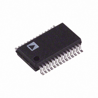
AD5554BRS Analog Devices Inc, AD5554BRS Datasheet - Page 7

AD5554BRS
Manufacturer Part Number
AD5554BRS
Description
IC DAC 14BIT QUAD SERIAL 28-SSOP
Manufacturer
Analog Devices Inc
Datasheet
1.AD5554BRSZ.pdf
(16 pages)
Specifications of AD5554BRS
Rohs Status
RoHS non-compliant
Settling Time
2µs
Number Of Bits
14
Data Interface
Serial
Number Of Converters
4
Voltage Supply Source
Dual ±
Power Dissipation (max)
1.25mW
Operating Temperature
-40°C ~ 85°C
Mounting Type
Surface Mount
Package / Case
28-SSOP
Available stocks
Company
Part Number
Manufacturer
Quantity
Price
Part Number:
AD5554BRSZ
Manufacturer:
ADI/亚德诺
Quantity:
20 000
PIN CONFIGURATION AND FUNCTION DESCRIPTIONS
Table 4. Pin Function Descriptions
Pin No.
1
2
3
4
5
6
7
8
9
10
11
12
13
14
15
16
17
18
19
20
21
22
23
24
25
26
27
28
Mnemonic
A
I
V
R
MSB
RS
V
CS
CLK
SDI
R
V
I
A
A
I
V
R
NC
SDO
LDAC
A
V
DGND
R
V
I
A
OUT
OUT
OUT
OUT
FB
FB
FB
FB
GND
REF
DD
REF
GND
GND
REF
GND
SS
REF
GND
A
B
C
D
A
B
C
D
A
B
C
D
A
B
C
F
D
Description
DAC A Analog Ground.
DAC A Current Output.
DAC A Reference Voltage Input Terminal. Establishes DAC A full-scale output voltage. Pin can be tied to the V
Establish voltage output for DAC A by connecting to external amplifier output.
MSB Bit. Set pin during a reset pulse (RS) or at system power-on if tied to ground or V
Reset Pin, Active Low Input. Input registers and DAC registers are set to all 0s or half-scale code (0x8000 for the
AD5544 and 0x2000 for the AD5554), determined by the voltage on the MSB pin. Register data = 0x0000 when
MSB = 0.
Positive Power Supply Input. Specified range of operation: 5 V ± 10%.
Chip Select, Active Low Input. Disables shift register loading when high. Transfers serial register data to the input
register when CS/LDAC returns high. Does not affect LDAC operation.
Clock Input. Positive edge clocks data into shift register.
Serial Data Input. Input data loads directly into the shift register.
Establish voltage output for DAC B by connecting to external amplifier output.
DAC B Reference Voltage Input Terminal. Establishes DAC B full-scale output voltage. Pin can be tied to the V
DAC B Current Output.
DAC B Analog Ground.
DAC C Analog Ground.
DAC C Current Output.
DAC C Reference Voltage Input Terminal. Establishes DAC C full-scale output voltage. Pin can be tied to the V
Establish voltage output for DAC C by connecting to external amplifier output.
No Connect. Leave pin unconnected.
Serial Data Output. Input data loads directly into the shift register. Data appears at SDO at 19 clock pulses for the
AD5544 and 17 clock pulses for the AD5554 after input at the SDI pin.
Load DAC Register Strobe, Level Sensitive Active Low. Transfers all input register data to DAC registers.
Asynchronous active low input. See Table 8 and Table 9 for operation.
High Current Analog Force Ground.
Negative Bias Power Supply Input. Specified range of operation: −5.5 V to +0.3 V.
Digital Ground Pin.
Establish voltage output for DAC D by connecting to external amplifier output.
DAC D Reference Voltage Input Terminal. Establishes DAC D full-scale output voltage. Pin can be tied to the V
DAC D Current Output.
DAC D Analog Ground.
A
A
V
V
I
I
GND
R
R
GND
OUT
OUT
REF
REF
MSB
CLK
FB
V
FB
SDI
CS
RS
DD
Figure 5. Pin Configuration
A
A
A
A
B
B
B
B
10
11
12
13
14
NC = NO CONNECT
1
2
3
4
5
6
7
8
9
Rev. D | Page 7 of 16
(Not to Scale)
AD5544/
AD5554
TOP VIEW
28
27
26
25
24
23
22
21
20
19
18
17
16
15
A
I
V
R
DGND
V
A
SDO
NC
R
V
I
A
LDAC
OUT
OUT
REF
SS
REF
GND
FB
GND
FB
GND
D
C
D
C
D
C
D
F
C
DD
AD5544/AD5554
.
DD
DD
pin.
DD
DD
pin.
pin.
pin.


