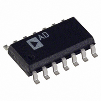
AD7394AR Analog Devices Inc, AD7394AR Datasheet - Page 10

AD7394AR
Manufacturer Part Number
AD7394AR
Description
IC DAC 12BIT SRL 3V 14-SOIC
Manufacturer
Analog Devices Inc
Datasheet
1.AD7394ARZ-REEL7.pdf
(12 pages)
Specifications of AD7394AR
Rohs Status
RoHS non-compliant
Settling Time
60µs
Number Of Bits
12
Data Interface
Serial
Number Of Converters
2
Voltage Supply Source
Single Supply
Power Dissipation (max)
1mW
Operating Temperature
-40°C ~ 85°C
Mounting Type
Surface Mount
Package / Case
14-SOIC (3.9mm Width), 14-SOL
Available stocks
Company
Part Number
Manufacturer
Quantity
Price
Part Number:
AD7394AR
Manufacturer:
ADI/亚德诺
Quantity:
20 000
Company:
Part Number:
AD7394ARZ
Manufacturer:
PANASONIC
Quantity:
560
Part Number:
AD7394ARZ
Manufacturer:
ADI/亚德诺
Quantity:
20 000
Part Number:
AD7394ARZ-REEL7
Manufacturer:
ADI/亚德诺
Quantity:
20 000
AD7394/AD7395
POWER SUPPLY
The very low power consumption of the AD7394/AD7395 is a
direct result of a circuit design optimizing the use of a CBCMOS
process. By using the low power characteristics of CMOS for
the logic, and the low noise, tight matching of the complemen-
tary bipolar transistors, excellent analog accuracy is achieved.
One advantage of the rail-to-rail output amplifiers used in the
AD7394/AD7395 is the wide range of usable supply voltage.
The part is fully specified and tested for operation from +2.7 V
to +5.5 V.
POWER SUPPLY BYPASSING AND GROUNDING
Local supply bypassing consisting of a 10 F tantalum electro-
lytic in parallel with a 0.1 F ceramic capacitor is recommended
in all applications (Figure 21).
INPUT LOGIC LEVELS
All digital inputs are protected with a Zener-type ESD protec-
tion structure (Figure 22) that allows logic input voltages to
exceed the V
user is driving one or more of the digital inputs with a 5 V CMOS
logic input-voltage level while operating the AD7394/AD7395
on a +3 V power supply. If this mode of interface is used, make
sure that the V
quirement of the AD7394/AD7395 operating at 3 V. See Figure
12 for a graph of digital logic input threshold versus operating
V
In order to minimize power dissipation from input logic levels
that are near the V
a Schmitt trigger design was used that minimizes the input-
buffer current consumption compared to traditional CMOS
input stages. Figure 11 is a plot of incremental input voltage
versus supply current showing that negligible current consump-
tion takes place when logic levels are in their quiescent state.
The normal crossover current still occurs during logic transi-
tions. A secondary advantage of this Schmitt trigger is the pre-
vention of false triggers that would occur with slow moving
DD
Figure 21. Recommended Supply Bypassing for the
AD7394/AD7395
Figure 22. Equivalent Digital Input ESD Protection
supply voltage.
*OPTIONAL EXTERNAL
REFERENCE BYPASS
LDA, B
CLK
SDI
CS
RS
DD
*
OL
supply voltage. This feature can be useful if the
LOGIC
of the 5 V CMOS meets the V
C
GND
IH
V
DD
IN
and V
REF
DGND
AD7394
AD7395
+2.7V TO +5.5V
IL
OR
logic input voltage specifications,
V
AGND
DD
0.1 F
IL
10 F
input re-
V
V
OUTA
OUTB
–10–
logic transitions when a standard CMOS logic interface or opto
isolators are used. The logic inputs SDI, CLK, CS, LDA, LDB,
RS, SHDN all contain the Schmitt trigger circuits.
DIGITAL INTERFACE
The AD7394/AD7395 has a serial data input. A functional
block diagram of the digital section is shown in Figure 23, while
Table I contains the truth table for the logic control inputs.
Three pins control the serial data input register loading. Two
additional pins determine which DAC will receive the data
loaded into the input shift register. Data at the SDI is clocked
into the shift register on the rising edge of the CLK. Data is
entered in the MSB-first format. The active low chip select (CS)
pin enables loading of data into the shift register from the SDI
pin. Twelve clock pulses are required to load the 12-bit AD7390
DAC shift register. If additional bits are clocked into the shift
register, for example, when a microcontroller sends two 8-bit
bytes, the MSBs are ignored (Table IV). The lowest resolution
AD7395 is also loaded MSB-first with 10 bits of data. Again, if
additional bits are clocked into the shift register only the last 10
bits clocked in are used. When CS returns to logic high, shift-
register loading is disabled. The load pins LDA and LDB con-
trol the flow of data from the shift register to the DAC register.
After a new value is clocked into the serial-input register, it will
be transferred to the DAC register associated with its LDA or
LDB logic control line. Note, if the user wants to load both
DAC registers with the current contents of the shift register,
both control lines LDA and LDB should be strobed together.
The LDA and LDB pins are level-sensitive and should be re-
turned to logic high prior to any new data being sent to the
input shift register to avoid changing the DAC register values.
See Truth Table for complete set of conditions.
RESET (RS) PIN
Forcing the asynchronous RS pin low will set the DAC register
to all zeros, or midscale, depending on the logic level applied to
the MSB pin. When the MSB pin is set to logic high, both DAC
registers will be reset to midscale (i.e., the DAC Register’s MSB
bit will be set to Logic 1 followed by all zeros). The reset func-
tion is useful for setting the DAC outputs to zero at power-up or
after a power supply interruption. Test systems and motor
controllers are two of many applications that benefit from
powering up to a known state. The external reset pulse can be
CLK
SDI
CS
Figure 23. Equivalent Digital Interface Logic
EN
REGISTER
SHIFT
Q
LDA LDB
DAC A REGISTER
DAC B REGISTER
D
D
P
P
R
R
RS MSB
REV. 0


