AD7568BS-REEL Analog Devices Inc, AD7568BS-REEL Datasheet - Page 3
AD7568BS-REEL
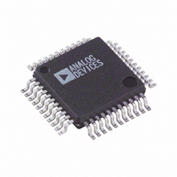
Manufacturer Part Number
AD7568BS-REEL
Description
IC DAC 12BIT OCTAL LC2MOS 44MQFP
Manufacturer
Analog Devices Inc
Datasheet
1.AD7568BPZ-REEL.pdf
(12 pages)
Specifications of AD7568BS-REEL
Rohs Status
RoHS non-compliant
Settling Time
500ns
Number Of Bits
12
Data Interface
Serial
Number Of Converters
8
Voltage Supply Source
Single Supply
Power Dissipation (max)
17.5mW
Operating Temperature
-40°C ~ 85°C
Mounting Type
Surface Mount
Package / Case
44-MQFP, 44-PQFP


REV. B
TIMING SPECIFICATIONS
Parameter
t
t
t
t
t
t
t
t
t
NOTES
1
2
Sample tested at +25 C to ensure compliance. All input signals are specified with tr = tf = 5 ns (10% to 90% of 5 V) and timed from a voltage level of 1.6 V.
t
1
2
3
4
5
6
7
8
9
8
2
is measured with the load circuit of Figure 2 and defined as the time required for the output to cross 0.8 V or 2.4 V.
Figure 2. Load Circuit for Digital Output
Timing Specifications
TO OUTPUT
PIN
50pF
C
L
Limit at
T
100
40
40
30
30
5
90
70
40
A
= +25 C
LDAC, CLR
SDOUT (O)
CLKIN (I)
1.6mA
200 A
FSIN (I)
SDIN (I)
NOTES
1. AO IS HARDWIRED HIGH OR LOW.
I
I
OL
OH
t
4
(V
t
6
DD
DB15
Limit at
T
100
40
40
30
30
5
90
70
40
= +5 V
A
= –40 C to +85 C
+2.1V
t
5
t
2
Figure 1. Timing Diagram
5%; I
OUT1
= I
t
t
t
1
7
8
OUT2
–3–
DB0
t
9
= 0 V; T
t
Model
AD7568BS
AD7568BP
*S = Plastic Quad Flatpack (PQFP), P = Plastic Leaded Chip Carrier (PLCC).
DB15
3
Units
ns min
ns min
ns min
ns min
ns min
ns min
ns min
ns max
ns min
A
= T
MIN
to T
Temperature
Range
–40 C to +85 C
–40 C to +85 C
MAX
, unless otherwise noted)
Description
CLKIN Cycle Time
CLKIN High Time
CLKIN Low Time
FSIN Setup Time
Data Setup Time
Data Hold Time
FSIN Hold Time
SDOUT Valid After CLKIN Falling Edge
LDAC, CLR Pulse Width
ORDERING GUIDE
DB0
Linearity
Error (LSBs)
0.5
0.5
AD7568
Package
Option*
S-44
P-44A
Related parts for AD7568BS-REEL
Image
Part Number
Description
Manufacturer
Datasheet
Request
R

Part Number:
Description:
IC DAC 12BIT LC2MOS OCTAL 44MQFP
Manufacturer:
Analog Devices Inc
Datasheet:

Part Number:
Description:
±1.7g Dual-Axis IMEMS Accelerometer Evaluation Board
Manufacturer:
Analog Devices Inc
Datasheet:

Part Number:
Description:
Inertial Sensor Evaluation System
Manufacturer:
Analog Devices Inc
Datasheet:
Part Number:
Description:
Manufacturer:
Analog Devices Inc
Datasheet:
Part Number:
Description:
Manufacturer:
Analog Devices Inc
Datasheet:
Part Number:
Description:
Manufacturer:
Analog Devices Inc
Datasheet:
Part Number:
Description:
Manufacturer:
Analog Devices Inc
Datasheet:
Part Number:
Description:
Manufacturer:
Analog Devices Inc
Datasheet:
Part Number:
Description:
Manufacturer:
Analog Devices Inc
Datasheet:
Part Number:
Description:
Manufacturer:
Analog Devices Inc
Datasheet:
Part Number:
Description:
Manufacturer:
Analog Devices Inc
Datasheet:
Part Number:
Description:
Manufacturer:
Analog Devices Inc
Datasheet:
Part Number:
Description:
Manufacturer:
Analog Devices Inc
Datasheet: