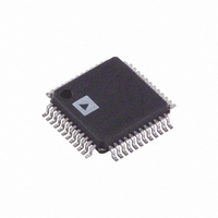
AD9709ASTRL Analog Devices Inc, AD9709ASTRL Datasheet - Page 3

AD9709ASTRL
Manufacturer Part Number
AD9709ASTRL
Description
IC DAC 8BIT DUAL 125MSPS 48-LQFP
Manufacturer
Analog Devices Inc
Series
TxDAC+®r
Datasheet
1.AD9709ASTZRL.pdf
(32 pages)
Specifications of AD9709ASTRL
Rohs Status
RoHS non-compliant
Settling Time
35ns
Number Of Bits
8
Data Interface
Parallel
Number Of Converters
2
Voltage Supply Source
Analog and Digital
Power Dissipation (max)
450mW
Operating Temperature
-40°C ~ 85°C
Mounting Type
Surface Mount
Package / Case
48-LQFP
For Use With
AD9709-EBZ - BOARD EVAL FOR AD9709
SPECIFICATIONS
DC SPECIFICATIONS
T
Table 1.
Parameter
RESOLUTION
DC ACCURACY
ANALOG OUTPUT
REFERENCE OUTPUT
REFERENCE INPUT
TEMPERATURE COEFFICIENTS
POWER SUPPLY
OPERATING RANGE
1
2
3
4
5
6
7
Measured at I
Nominal full-scale current, I
An external buffer amplifier with input bias current <100 nA should be used to drive any external load.
Measured at f
Measured at f
Measured as unbuffered voltage output with I
±10% power supply variation.
MIN
Integral Linearity Error (INL)
Differential Nonlinearity (DNL)
Offset Error
Gain Error Without Internal Reference
Gain Error with Internal Reference
Gain Match
Full-Scale Output Current
Output Compliance Range
Output Resistance
Output Capacitance
Reference Voltage
Reference Output Current
Input Compliance Range
Reference Input Resistance
Small-Signal Bandwidth
Offset Drift
Gain Drift Without Internal Reference
Gain Drift with Internal Reference
Reference Voltage Drift
Supply Voltages
AVDD
DVDD1, DVDD2
Analog Supply Current (I
Digital Supply Current (I
Digital Supply Current (I
Supply Current Sleep Mode (I
Power Dissipation
Power Dissipation
Power Dissipation
Power Supply Rejection Ratio
Power Supply Rejection Ratio
to T
T
T
T
A
MIN
MIN
= 25°C
MAX
to T
to T
OUTA
CLK
CLK
, AVDD = 3.3 V or 5 V, DVDD1 = DVDD2 = 3.3 V or 5 V, I
MAX
MAX
1
= 25 MSPS and f
= 100 MSPS and f
, driving a virtual ground.
4
5
6
(5 V, I
(5 V, I
(5 V, I
OUTFS
DVDD
DVDD
OUTFS
OUTFS
AVDD
OUTFS
, is 32 times the I
2
OUT
3
OUT
)
)
)
= 1.0 MHz.
4
5
= 20 mA)
= 20 mA)
AVDD
= 20 mA)
= 1 MHz.
7
7
—DVDD1, DVDD2
—AVDD
)
OUTFS
REF
current.
= 20 mA and R
LOAD
= 50 Ω at I
Rev. B | Page 3 of 32
OUTA
and I
Min
8
−0.5
−0.5
−0.02
−2
−5
−0.3
−1.6
−0.14
2.0
−1.0
1.14
0.1
3
2.7
−0.4
−0.025
−40
OUTFS
OUTB
, f
= 20 mA, unless otherwise noted.
CLK
= 100 MSPS, and f
Typ
±0.1
±0.25
±0.1
100
5
1.20
100
1
±50
±50
5
5
71
5
8
±0.1
+1
0.5
0
±100
380
420
450
OUT
Max
+0.5
+0.5
+0.02
+2
+5
+0.3
+1.6
+0.14
20.0
+1.25
1.26
1.25
5.5
5.5
75
7
15
12
410
450
+0.4
+0.025
+85
= 40 MHz.
Unit
Bits
LSB
LSB
% of FSR
% of FSR
% of FSR
% of FSR
% of FSR
dB
mA
V
kΩ
pF
V
nA
V
MΩ
MHz
ppm of FSR/°C
ppm of FSR/°C
ppm of FSR/°C
ppm/°C
V
V
mA
mA
mA
mA
mW
mW
mW
% of FSR/V
% of FSR/V
°C
AD9709


