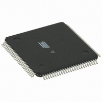
ATF1504ASVL-20AU100 Atmel, ATF1504ASVL-20AU100 Datasheet - Page 15

ATF1504ASVL-20AU100
Manufacturer Part Number
ATF1504ASVL-20AU100
Description
IC CPLD 20NS LOWV LOWPWR 100TQFP
Manufacturer
Atmel
Series
ATF1504ASV(L)r
Datasheet
1.ATF1504ASV-15JU44.pdf
(31 pages)
Specifications of ATF1504ASVL-20AU100
Programmable Type
In System Programmable (min 10K program/erase cycles)
Delay Time Tpd(1) Max
20.0ns
Voltage Supply - Internal
3 V ~ 3.6 V
Number Of Macrocells
64
Number Of I /o
64
Operating Temperature
-40°C ~ 85°C
Mounting Type
Surface Mount
Package / Case
100-TQFP, 100-VQFP
Voltage
3.3V
Memory Type
EEPROM
Number Of Product Terms Per Macro
40
Maximum Operating Frequency
66 MHz
Delay Time
20 ns
Number Of Programmable I/os
64
Operating Supply Voltage
3.3 V
Maximum Operating Temperature
+ 85 C
Minimum Operating Temperature
- 40 C
Mounting Style
SMD/SMT
Supply Voltage (max)
3.6 V
Supply Voltage (min)
3 V
For Use With
ATF15XX-DK3 - KIT DEV FOR ATF15XX CPLD'S
Lead Free Status / RoHS Status
Lead free / RoHS Compliant
Features
-
Number Of Logic Elements/cells
-
Lead Free Status / Rohs Status
Details
Available stocks
Company
Part Number
Manufacturer
Quantity
Price
Part Number:
ATF1504ASVL-20AU100
Manufacturer:
ATMEL/爱特梅尔
Quantity:
20 000
Power-down Mode
Power Down AC Characteristics
Notes:
1409J–PLD–6/05
Symbol
t
t
t
t
t
t
t
t
t
t
IVDH
GVDH
CVDH
DHIX
DHGX
DHCX
DLIV
DLGV
DLCV
DLOV
1. For slow slew outputs, add t
2. Pin or product term.
3. Includes t
Parameter
Valid I, I/O before PD High
Valid OE
Valid Clock
I, I/O Don’t Care after PD High
OE
Clock
PD Low to Valid I, I/O
PD Low to Valid OE (Pin or Term)
PD Low to Valid Clock (Pin or Term)
PD Low to Valid Output
(2)
(2)
Don’t Care after PD High
Don’t Care after PD High
(2)
RPA
(2)
before PD High
for reduced-power bit enabled.
before PD High
The ATF1504ASV(L) includes an optional pin-controlled power-down feature. When this
mode is enabled, the PD pin acts as the power-down pin. When the PD pin is high, the
device supply current is reduced to less than 3 mA. During power down, all output data
and internal logic states are latched internally and held. Therefore, all registered and
combinatorial output data remain valid. Any outputs that were in a High-Z state at the
onset will remain at High-Z. During power down, all input signals except the power-down
pin are blocked. Input and I/O hold latches remain active to ensure that pins do not float
to indeterminate levels, further reducing system power. The power-down mode feature
is enabled in the logic design file or as a fitted or translated s/w option. Designs using
the power-down pin may not use the PD pin as a logic array input. However, all other PD
pin macrocell resources may still be used, including the buried feedback and foldback
product term array inputs.
SSO
.
(1)(2)
Min
15
15
15
-15
Max
25
25
25
1
1
1
1
Min
20
20
20
ATF1504ASV(L)
-20
Max
30
30
30
1
1
1
1
Units
ns
ns
ns
ns
ns
ns
µs
µs
µs
µs
15


