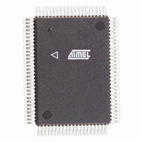
ATF1508AS-10QU100 Atmel, ATF1508AS-10QU100 Datasheet - Page 7

ATF1508AS-10QU100
Manufacturer Part Number
ATF1508AS-10QU100
Description
IC CPLD 10NS 100PQFP
Manufacturer
Atmel
Series
ATF1508AS(L)r
Datasheet
1.ATF1508ASL-20JC84.pdf
(31 pages)
Specifications of ATF1508AS-10QU100
Programmable Type
In System Programmable (min 10K program/erase cycles)
Delay Time Tpd(1) Max
10.0ns
Voltage Supply - Internal
4.5 V ~ 5.5 V
Number Of Macrocells
128
Number Of I /o
80
Operating Temperature
-40°C ~ 85°C
Mounting Type
Surface Mount
Package / Case
100-MQFP, 100-PQFP
Voltage
5V
Memory Type
EEPROM
Number Of Product Terms Per Macro
40
Maximum Operating Frequency
125 MHz
Delay Time
10 ns
Number Of Programmable I/os
80
Operating Supply Voltage
5 V
Maximum Operating Temperature
+ 85 C
Minimum Operating Temperature
- 40 C
Mounting Style
SMD/SMT
Supply Voltage (max)
5.5 V
Supply Voltage (min)
4.5 V
For Use With
ATF15XX-DK3 - KIT DEV FOR ATF15XX CPLD'S
Lead Free Status / RoHS Status
Lead free / RoHS Compliant
Features
-
Number Of Logic Elements/cells
-
Lead Free Status / Rohs Status
Lead free / RoHS Compliant
Available stocks
Company
Part Number
Manufacturer
Quantity
Price
Part Number:
ATF1508AS-10QU100
Manufacturer:
ATMEL/爱特梅尔
Quantity:
20 000
Speed/Power
Management
I/O Diagram
0784P–PLD–7/05
The ATF1508AS has several built-in speed and power management features. The
ATF1508AS contains circuitry that automatically puts the device into a low-power stand-by
mode when no logic transitions are occurring. This not only reduces power consumption dur-
ing inactive periods, but also provides proportional power-savings for most applications
running at system speeds below 5 MHz.
To further reduce power, each ATF1508AS macrocell has a Reduced-power bit feature. This
feature allows individual macrocells to be configured for maximum power savings. This feature
may be selected as a design option.
All ATF1508 also have an optional power-down mode. In this mode, current drops to below 10
mA. When the power-down option is selected, either PD1 or PD2 pins (or both) can be used to
power down the part. The power-down option is selected in the design source file. When
enabled, the device goes into power-down when either PD1 or PD2 is high. In the power-down
mode, all internal logic signals are latched and held, as are any enabled outputs.
All pin transitions are ignored until the PD pin is brought low. When the power-down feature is
enabled, the PD1 or PD2 pin cannot be used as a logic input or output. However, the pin’s
macrocell may still be used to generate buried foldback and cascade logic signals.
All power-down AC characteristic parameters are computed from external input or I/O pins,
with Reduced-power Bit turned on. For macrocells in reduced-power mode (Reduced-power
bit turned on), the reduced-power adder, tRPA, must be added to the AC parameters, which
include the data paths t
Each output also has individual slew rate control. This may be used to reduce system noise by
slowing down outputs that do not need to operate at maximum speed. Outputs default to slow
switching, and may be specified as fast switching in the design file.
LAD
, t
LAC
, t
IC
, t
ACL
, t
ACH
and t
SEXP
.
ATF1508AS(L)
7


