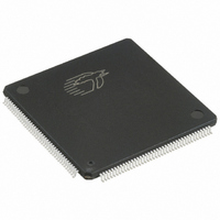
CY37128P160-125AXI Cypress Semiconductor Corp, CY37128P160-125AXI Datasheet - Page 7

CY37128P160-125AXI
Manufacturer Part Number
CY37128P160-125AXI
Description
IC CPLD 128 MACROCELL 160LQFP
Manufacturer
Cypress Semiconductor Corp
Series
Ultra37000™r
Specifications of CY37128P160-125AXI
Programmable Type
In-System Reprogrammable™ (ISR™) CMOS
Delay Time Tpd(1) Max
10.0ns
Voltage Supply - Internal
4.5 V ~ 5.5 V
Number Of Macrocells
128
Number Of I /o
133
Operating Temperature
-40°C ~ 85°C
Mounting Type
Surface Mount
Package / Case
160-LQFP
Voltage
5V
Memory Type
CMOS
Family Name
Ultra 37000
# Macrocells
128
Number Of Usable Gates
3800
Frequency (max)
125MHz
Propagation Delay Time
10ns
Number Of Logic Blocks/elements
8
# I/os (max)
133
Operating Supply Voltage (typ)
5V
In System Programmable
Yes
Operating Supply Voltage (min)
4.5V
Operating Supply Voltage (max)
5.5V
Operating Temp Range
-40C to 85C
Operating Temperature Classification
Industrial
Mounting
Surface Mount
Pin Count
160
Package Type
TQFP
Lead Free Status / RoHS Status
Lead free / RoHS Compliant
For Use With
CY3710 - ADAPTER SOCKET PTG
Features
-
Number Of Logic Elements/cells
-
Lead Free Status / RoHS Status
Compliant, Lead free / RoHS Compliant
Available stocks
Company
Part Number
Manufacturer
Quantity
Price
Company:
Part Number:
CY37128P160-125AXI
Manufacturer:
Cypress Semiconductor Corp
Quantity:
10 000
Company:
Part Number:
CY37128P160-125AXIT
Manufacturer:
Cypress Semiconductor Corp
Quantity:
10 000
Clocking
Each I/O and buried macrocell has access to four synchronous
clocks (CLK0, CLK1, CLK2 and CLK3) and an asynchronous
product term clock PTCLK. Each input macrocell has access to
all four synchronous clocks.
Dedicated Inputs/Clocks
Five pins on each member of the Ultra37000 family are
designated as input-only. There are two types of dedicated
inputs on Ultra37000 devices: input pins and input/clock pins.
Figure 3
options are available for the user: combinatorial, registered,
double-registered, or latched. If a registered or latched option is
selected, any one of the input clocks can be selected for control.
Figure 4
Similar to the input pins, input/clock pins can be combinatorial,
registered, double-registered, or latched. In addition, these pins
feed the clocking structures throughout the device. The clock
path at the input has user-configurable polarity.
Product Term Clocking
In addition to the four synchronous clocks, the Ultra37000 family
also has a product term clock for asynchronous clocking. Each
logic block has an independent product term clock which is
available to all 16 macrocells. Each product term clock also
supports user configurable polarity selection.
Timing Model
One of the most important features of the Ultra37000 family is
the simplicity of its timing. All delays are worst case and system
performance is unaffected by the features used.
illustrates the true timing model for the 167-MHz devices in high
speed mode. For combinatorial paths, any input to any output
incurs a 6.5 ns worst-case delay regardless of the amount of
logic used. For synchronous systems, the input setup time to the
output macrocells for any input is 3.5 ns and the clock to output
time is also 4.0 ns. These measurements are for any output and
synchronous clock, regardless of the logic used.
Document Number : 38-03007 Rev. *H
POLARITY INPUT
FROM CLOCK
CLOCK PINS
illustrates the architecture for input pins. Four input
illustrates the architecture for the input/clock pins.
INPUT/CLOCK PIN
0
1
2
3
C8 C9
O
D
D
LE
Q
Q
Figure 4. Input/Clock Macrocell
D
Figure 5
Q
0
1
The Ultra37000 features:
■
■
■
■
■
■
■
■
■
The simple timing model of the Ultra37000 family eliminates
unexpected performance penalties.
INPUT
INPUT
CLOCK
C12
No fanout delays
No expander delays
No dedicated vs. I/O pin delays
No additional delay through PIM
No penalty for using 0–16 product terms
No added delay for steering product terms
No added delay for sharing product terms
No routing delays
No output bypass delays
0
1
2
3
C10C11
O
t
S
O
= 3.5 ns
Figure 5. Timing Model for CY37128
TO PIM
COMBINATORIAL SIGNAL
REGISTERED SIGNAL
TO CLOCK MUX ON
ALL INPUT MACROCELLS
Ultra37000 CPLD Family
C13, C14, C15
t
PD
D,T,L
= 6.5 ns
0
1
O
O
CLOCK POLARITY MUX
ONE PER LOGIC BLOCK
FOR EACH CLOCK INPUT
OR C16
t
CO
= 4.5 ns
TO CLOCK MUX
IN EACH
LOGIC BLOCK
Page 7 of 43
OUTPUT
OUTPUT
[+] Feedback


