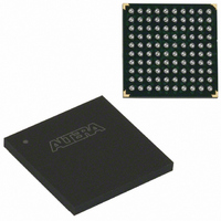
EPM570GF100C5N Altera, EPM570GF100C5N Datasheet - Page 25

EPM570GF100C5N
Manufacturer Part Number
EPM570GF100C5N
Description
IC MAX II CPLD 570 LE 100-FBGA
Manufacturer
Altera
Series
MAX® IIr
Datasheets
1.EPM240GT100C5N.pdf
(6 pages)
2.EPM240GT100C5N.pdf
(88 pages)
3.EPM240GM100C5N.pdf
(10 pages)
Specifications of EPM570GF100C5N
Programmable Type
In System Programmable
Delay Time Tpd(1) Max
5.4ns
Voltage Supply - Internal
1.71 V ~ 1.89 V
Number Of Logic Elements/blocks
570
Number Of Macrocells
440
Number Of I /o
76
Operating Temperature
0°C ~ 85°C
Mounting Type
Surface Mount
Package / Case
100-FBGA
Voltage
1.8V
Memory Type
FLASH
Number Of Logic Elements/cells
570
Lead Free Status / RoHS Status
Lead free / RoHS Compliant
Features
-
Other names
544-1730
Available stocks
Company
Part Number
Manufacturer
Quantity
Price
Chapter 2: MAX II Architecture
Global Signals
© October 2008 Altera Corporation
Figure 2–13. Global Clock Generation
Note to
(1) Any I/O pin can use a MultiTrack interconnect to route as a logic array-generated global clock signal.
The global clock network drives to individual LAB column signals, LAB column
clocks [3..0], that span an entire LAB column from the top to the bottom of the device.
Unused global clocks or control signals in a LAB column are turned off at the LAB
column clock buffers shown in
multiplexed down to two LAB clock signals and one LAB clear signal. Other control
signal types route from the global clock network into the LAB local interconnect. See
“LAB Control Signals” on page 2–5
Figure 2–13
:
Logic Array(1)
GCLK0
GCLK1
GCLK2
GCLK3
Figure
for more information.
4
2–14. The LAB column clocks [3..0] are
4
Global Clock
Network
MAX II Device Handbook
2–17


