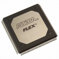
EPM9560RI240-20 Altera, EPM9560RI240-20 Datasheet - Page 9

EPM9560RI240-20
Manufacturer Part Number
EPM9560RI240-20
Description
IC MAX 9000 CPLD 560 240-RQFP
Manufacturer
Altera
Series
MAX® 9000r
Datasheet
1.EPM9320LC84-15.pdf
(46 pages)
Specifications of EPM9560RI240-20
Programmable Type
In System Programmable
Delay Time Tpd(1) Max
20.0ns
Voltage Supply - Internal
4.5 V ~ 5.5 V
Number Of Logic Elements/blocks
35
Number Of Macrocells
560
Number Of Gates
12000
Number Of I /o
191
Operating Temperature
-40°C ~ 85°C
Mounting Type
Surface Mount
Package / Case
240-RQFP
Voltage
3.3V/5V
Memory Type
EEPROM
Number Of Logic Elements/cells
35
Lead Free Status / RoHS Status
Contains lead / RoHS non-compliant
Features
-
Other names
544-2367
Available stocks
Company
Part Number
Manufacturer
Quantity
Price
Company:
Part Number:
EPM9560RI240-20
Manufacturer:
SYNCMOS
Quantity:
400
Company:
Part Number:
EPM9560RI240-20
Manufacturer:
ALTERA
Quantity:
49
Part Number:
EPM9560RI240-20
Manufacturer:
ALTERA/阿尔特拉
Quantity:
20 000
Altera Corporation
For registered functions, each macrocell register can be individually
programmed for D, T, JK, or SR operation with programmable clock
control. The flipflop can also be bypassed for combinatorial operation.
During design entry, the user specifies the desired register type; the
MAX+PLUS II software then selects the most efficient register operation
for each registered function to optimize resource utilization.
Each programmable register can be clocked in three different modes:
Two global clock signals are available. As shown in
clock signals can be the true or the complement of either of the global clock
pins (DIN1 and DIN2).
Each register also supports asynchronous preset and clear functions. As
shown in
to control these operations. Although the product-term-driven preset and
clear inputs to registers are active high, active-low control can be obtained
by inverting the signal within the logic array. In addition, each register
clear function can be individually driven by the dedicated global clear pin
(DIN3). The global clear can be programmed for active-high or active-low
operation.
All MAX 9000 macrocells offer a dual-output structure that provides
independent register and combinatorial logic output within the same
macrocell. This function is implemented by a process called register
packing. When register packing is used, the product-term select matrix
allocates one product term to the D input of the register, while the
remaining product terms can be used to implement unrelated
combinatorial logic. Both the registered and the combinatorial output of
the macrocell can feed either the FastTrack Interconnect or the LAB local
array.
By either global clock signal. This mode achieves the fastest clock-to-
output performance.
By a global clock signal and enabled by an active-high clock enable.
This mode provides an enable on each flipflop while still achieving
the fast clock-to-output performance of the global clock.
By an array clock implemented with a product term. In this mode, the
flipflop can be clocked by signals from buried macrocells or I/O pins.
Figure
3, the product-term select matrix allocates product terms
MAX 9000 Programmable Logic Device Family Data Sheet
Figure
2, these global
9


