XC95144XL-7TQG144I Xilinx Inc, XC95144XL-7TQG144I Datasheet
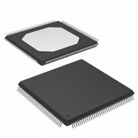
IC CPLD 144MCELL 7.5NS 144-TQFP

XC95144XL-7TQG144I

Manufacturer Part Number
XC95144XL-7TQG144I
Description
IC CPLD 144MCELL 7.5NS 144-TQFP
Manufacturer
Xilinx Inc
Series
XC9500XLr

Specifications of XC95144XL-7TQG144I

Programmable Type
In System Programmable (min 10K program/erase cycles)
Delay Time Tpd(1) Max
7.5ns
Voltage Supply - Internal
3 V ~ 3.6 V
Number Of Logic Elements/blocks
8
Number Of Macrocells
144
Number Of Gates
3200
Number Of I /o
117
Operating Temperature
-40°C ~ 85°C
Mounting Type
Surface Mount
Package / Case
144-TQFP, 144-VQFP
Features
Automotive
Voltage
3.0 V ~ 3.6 V
Memory Type
CMOS
Package
144TQFP
Family Name
XC9500XL
Device System Gates
3200
Maximum Propagation Delay Time
7.5 ns
Number Of User I/os
117
Number Of Logic Blocks/elements
8
Typical Operating Supply Voltage
3.3 V
Maximum Operating Frequency
125 MHz
Number Of Product Terms Per Macro
90
Lead Free Status / RoHS Status
Lead free / RoHS Compliant
Number Of Logic Elements/cells
-

Available stocks

Company
Part Number
Manufacturer
Quantity
Price
Part Number:
XC95144XL-7TQG144I
Manufacturer:
XILINX
Quantity:
40
Part Number:
XC95144XL-7TQG144I
Manufacturer:
Xilinx Inc
Quantity:
10 000
Part Number:
XC95144XL-7TQG144I
Manufacturer:
XILINX
0
DS056 (v2.0) April 3, 2007
Features
WARNING: Programming temperature range of
T
Description
The XC95144XL is a 3.3V CPLD targeted for high-perfor-
mance, low-voltage applications in leading-edge communi-
cations and computing systems. It is comprised of eight
DS056 (v2.0) April 3, 2007
Product Specification
A
= 0° C to +70° C
© 1998-2007 Xilinx, Inc. All rights reserved. All Xilinx trademarks, registered trademarks, patents, and disclaimers are as listed at http://www.xilinx.com/legal.htm.
5 ns pin-to-pin logic delays
System frequency up to 178 MHz
144 macrocells with 3,200 usable gates
Available in small footprint packages
-
-
-
-
Optimized for high-performance 3.3V systems
-
-
-
-
Advanced system features
-
-
-
-
-
-
-
-
-
Fast concurrent programming
Slew rate control on individual outputs
Enhanced data security features
Excellent quality and reliability
-
-
-
Pin-compatible with 5V-core XC95144 device in the
100-pin TQFP package
100-pin TQFP (81 user I/O pins)
144-pin TQFP (117 user I/O pins)
144-CSP (117 user I/O pins)
Pb-free available for all packages
Low power operation
5V tolerant I/O pins accept 5V, 3.3V, and 2.5V
signals
3.3V or 2.5V output capability
Advanced 0.35 micron feature size CMOS
Fast FLASH™ technology
In-system programmable
Superior pin-locking and routability with
Fast CONNECT™ II switch matrix
Extra wide 54-input Function Blocks
Up to 90 product-terms per macrocell with
individual product-term allocation
Local clock inversion with three global and one
product-term clocks
Individual output enable per output pin with local
inversion
Input hysteresis on all user and boundary-scan pin
inputs
Bus-hold circuitry on all user pin inputs
Full IEEE Standard 1149.1 boundary-scan (JTAG)
Endurance exceeding 10,000 program/erase
cycles
20 year data retention
ESD protection exceeding 2,000V
All other trademarks and registered trademarks are the property of their respective owners. All specifications are subject to change without notice.
R
0
0
www.xilinx.com
0
XC95144XL High Performance
CPLD
Product Specification
54V18 Function Blocks, providing 3,200 usable gates with
propagation delays of 5 ns. See
Power Estimation
Power dissipation in CPLDs can vary substantially depend-
ing on the system frequency, design application and output
loading. To help reduce power dissipation, each macrocell
in a XC9500XL device may be configured for low-power
mode (from the default high-performance mode). In addi-
tion, unused product-terms and macrocells are automati-
cally deactivated by the software to further conserve power.
For a general estimate of I
used:
I
where:
This calculation was derived from laboratory measurements
of an XC9500XL part filled with 16-bit counters and allowing
a single output (the LSB) to be enabled. The actual I
value varies with the design application and should be veri-
fied during normal system operation.
above estimation in a graphical form. For a more detailed
discussion of power consumption in this device, see Xilinx
CC
(mA) = MC
MC
PT
per macrocell
MC
PT
macrocell
f = maximum clock frequency
MCTOG = average % of flip-flops toggling per clock
(~12%)
HS
LP
HS
LP
+ 0.272) + 0.04 * MC
= average number of low power product terms per
= average number of high-speed product terms
= # macrocells in low power configuration
= # macrocells in high-speed configuration
HS
(0.175*PT
CC
HS
, the following equation may be
TOG
+ 0.345) + MC
Figure 2
(MC
HS
Figure 1
+MC
for overview.
LP
LP
(0.052*PT
)* f
shows the
LP
CC
1

Related parts for XC95144XL-7TQG144I

XC95144XL-7TQG144I Summary of contents

Page 1

... C to +70° Description The XC95144XL is a 3.3V CPLD targeted for high-perfor- mance, low-voltage applications in leading-edge communi- cations and computing systems comprised of eight © 1998-2007 Xilinx, Inc. All rights reserved. All Xilinx trademarks, registered trademarks, patents, and disclaimers are as listed at http://www.xilinx.com/legal.htm. ...

Page 2

... XC95144XL High Performance CPLD application note XAPP114, “Understanding XC9500XL CPLD Power.” 250 200 150 104 MHz 100 100 Clock Frequency (MHz) Figure 1: Typical I vs. Frequency for XC95144XL CC 2 178 MHz 150 200 www.xilinx.com R DS056 (v2.0) April 3, 2007 Product Specification ...

Page 3

... I/O/GSR 4 I/O/GTS Function Block outputs (indicated by the bold line) drive the I/O Blocks directly. DS056 (v2.0) April 3, 2007 Product Specification JTAG In-System Programming Controller Controller I/O Blocks Figure 2: XC95144XL Architecture www.xilinx.com XC95144XL High Performance CPLD 54 Function 18 Block 1 Macrocells Function 18 Block 2 Macrocells ...

Page 4

... XC95144XL High Performance CPLD Absolute Maximum Ratings Symbol V Supply voltage relative to GND CC V Input voltage relative to GND IN V Voltage applied to 3-state output TS T Storage temperature (ambient) STG T Junction temperature J Notes: 1. Maximum DC undershoot below GND must be limited to either 0. mA, whichever is easier to achieve. During transitions, the device pins may undershoot to – ...

Page 5

... Output Type V CCIO 3.3V 2. Figure 3: AC Load Circuit www.xilinx.com XC95144XL High Performance CPLD Min Max - ±10 - ± (Typical) XC95144XL-7 XC95144XL-10 Min Max Min Max - 7.5 - 10.0 4 4.5 - 5.8 - 125.0 - 100 ...

Page 6

... XC95144XL High Performance CPLD Internal Timing Parameters Symbol Parameter Buffer Delays T Input buffer delay IN T GCK buffer delay GCK T GSR buffer delay GSR T GTS buffer delay GTS T Output buffer delay OUT T Output buffer enable/disable EN delay Product Term Control Delays T Product term clock delay ...

Page 7

... C3 375 4 (1) (1) A2 372 369 366 4 (1) ( 363 4 (1) ( 360 357 4 (1) ( 354 4 (1) ( 351 348 345 342 339 336 333 330 327 324 4 www.xilinx.com XC95144XL High Performance CPLD Macro- cell TQ100 TQ144 CS144 (1) (1) (1) ( (1) (1) (1) ( 118 ...

Page 8

... XC95144XL High Performance CPLD XC95144XL (Continued) Function Macro- Block cell TQ100 TQ144 CS144 – Notes: 1. The pin-outs are the same for Pb-free versions of packages. 8 BScan Function Order Block - - 213 210 207 204 201 198 7 66 M10 195 192 189 7 68 N11 ...

Page 9

... R XC95144XL Global, JTAG and Power Pins Pin Type TQ100 I/O/GCK1 I/O/GCK2 I/O/GCK3 I/O/GTS1 I/O/GTS2 I/O/GTS3 I/O/GTS4 I/O/GSR TCK TDI TDO TMS V 3.3V 5, 57, 98 CCINT V 2.5V/3.3V 26, 38, 51, 88 CCIO GND 21, 31, 44, 62, 69, 75, 84, 100 No Connects Notes: 1. The pin-outs are the same for Pb-free versions of packages. ...

Page 10

... XC95144XL-10TQ144I 10 ns XC95144XL-10CS144I 10 ns XC95144XL-5TQG100C 5 ns XC95144XL-5TQG144C 5 ns XC95144XL-5CSG144C 5 ns XC95144XL-7TQG100C 7.5 ns XC95144XL-7TQG144C 7.5 ns XC95144XL-7CSG144C 7.5 ns XC95144XL-7TQG100I 7.5 ns XC95144XL-7TQG144I 7.5 ns XC95144XL-7CSG144I 7 XC95xxxXL TQ144 7C 1 Sample package with part marking. Pkg. No. of Symbol Pins TQ100 100-pin Thin Quad Flat Pack (TQFP) TQ144 ...

Page 11

... TQG100 100-pin Thin Quad Flat Pack (TQFP); Pb-free TQG144 144-pin Thin Quad Flat Pack (TQFP); Pb-free CSG144 144-ball Chip Scale Package (CSP); Pb-free = –40° to +85°C A Pb- Free Example: XC95144XL 144 C Device Speed Grade Package Type Pb -Free Number of Pins Temperature Range www ...

Page 12

... XC95144XL High Performance CPLD Revision History The following table shows the revision history for this document. Date Version 10/30/98 1.1 Minor corrections to CS144 pinout table. 11/13/98 1.2 V1.2 minor correction in CS144 pinout table. 06/20/02 1.3 Updated I Component Availability chart.Added additional I Characteristics table. ...

Related keywords