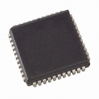
ATF1502ASV-15JC44 Atmel, ATF1502ASV-15JC44 Datasheet - Page 7

ATF1502ASV-15JC44
Manufacturer Part Number
ATF1502ASV-15JC44
Description
IC CPLD 32 MACROCELL LV 44PLCC
Manufacturer
Atmel
Series
ATF1502ASVr
Datasheet
1.ATF1502ASV-15AU44.pdf
(25 pages)
Specifications of ATF1502ASV-15JC44
Programmable Type
In System Programmable (min 10K program/erase cycles)
Delay Time Tpd(1) Max
15.0ns
Voltage Supply - Internal
3 V ~ 3.6 V
Number Of Macrocells
32
Number Of I /o
32
Operating Temperature
0°C ~ 70°C
Mounting Type
Surface Mount
Package / Case
44-PLCC
Voltage
3.0 V ~ 3.6 V
Memory Type
EEPROM
Lead Free Status / RoHS Status
Contains lead / RoHS non-compliant
Features
-
Number Of Logic Elements/cells
-
Available stocks
Company
Part Number
Manufacturer
Quantity
Price
Part Number:
ATF1502ASV-15JC44
Manufacturer:
ATMEL/爱特梅尔
Quantity:
20 000
4. Power-up Reset
5. Security Fuse Usage
6. Programming
1615J–PLD–01/06
All pin transitions are ignored until the PD pin is brought low. When the power-down feature is
enabled, the PD1 or PD2 pin cannot be used as a logic input or output. However, the pin’s mac-
rocell may still be used to generate buried foldback and cascade logic signals.
All power-down AC characteristic parameters are computed from external input or I/O pins, with
reduced-power bit turned on. For macrocells in reduced-power mode (reduced-power bit turned
on), the reduced-power adder, t
data paths t
The ATF1502ASV macrocell also has an option whereby the power can be reduced on a per-
macrocell basis. By enabling this power-down option, macrocells that are not used in an applica-
tion can be turned down, thereby reducing the overall power consumption of the device.
Each output also has individual slew rate control. This may be used to reduce system noise by
slowing down outputs that do not need to operate at maximum speed. Outputs default to slow
switching, and may be specified as fast switching in the design file.
The ATF1502ASV is designed with a power-up reset, a feature critical for state machine initial-
ization. At a point delayed slightly from V
state of each output will depend on the polarity of its buffer. However, due to the asynchronous
nature of reset and uncertainty of how V
are required:
The ATF1502ASV has two options for the hysteresis about the reset level, V
Large. To ensure a robust operating environment in applications where the device is operated
near 3.0V, Atmel recommends that during the fitting process users configure the device with the
Power-up Reset hysteresis set to Large. For conversions, Atmel POF2JED users should include
the flag “-power_reset” on the command line after “filename.POF”. To allow the registers to be
properly reinitialized with the Large hysteresis option selected, the following condition is added:
When the Large hysteresis option is active, I
well.
A single fuse is provided to prevent unauthorized copying of the ATF1502ASV fuse patterns.
Once programmed, fuse verify is inhibited. However, the 16-bit User Signature remains
accessible.
ATF1502ASV devices are in-system programmable (ISP) devices utilizing the 4-pin JTAG proto-
col. This capability eliminates package handling normally required for programming and
facilitates rapid design iterations and field changes.
1. The V
2. After reset occurs, all input and feedback setup times must be met before driving the
3. The clock must remain stable during T
4. If V
clock pin high, and,
CC
CC
LAD
falls below 2.0V, it must shut off completely before the device is turned on again.
rise must be monotonic,
, t
LAC
, t
IC
, t
ACL
, t
ACH
RPA
and t
, must be added to the AC parameters, which include the
SEXP
CC
CC
.
crossing V
actually rises in the system, the following conditions
D
.
CC
is reduced by several hundred microamps as
RST
, all registers will be initialized, and the
ATF1502ASV
RST
, Small and
7


