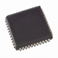
ATF2500C-15JI Atmel, ATF2500C-15JI Datasheet - Page 5

ATF2500C-15JI
Manufacturer Part Number
ATF2500C-15JI
Description
IC CPLD EE 15NS 44PLCC
Manufacturer
Atmel
Series
ATF2500C(L)r
Datasheet
1.ATF2500C-20JC.pdf
(24 pages)
Specifications of ATF2500C-15JI
Programmable Type
In System Programmable
Delay Time Tpd(1) Max
15.0ns
Voltage Supply - Internal
4.5 V ~ 5.5 V
Number Of Macrocells
24
Number Of I /o
24
Operating Temperature
-40°C ~ 85°C
Mounting Type
Surface Mount
Package / Case
44-PLCC
Voltage
5V
Memory Type
EEPROM
Family Name
ATF2500C
# Macrocells
24
Number Of Usable Gates
2500
Frequency (max)
83MHz
Propagation Delay Time
15ns
# I/os (max)
24
Operating Supply Voltage (typ)
5V
In System Programmable
No
Operating Supply Voltage (min)
4.5V
Operating Supply Voltage (max)
5.5V
Operating Temp Range
-40C to 85C
Operating Temperature Classification
Industrial
Mounting
Surface Mount
Pin Count
44
Package Type
PLCC
Lead Free Status / RoHS Status
Contains lead / RoHS non-compliant
Features
-
Number Of Logic Elements/cells
-
Lead Free Status / Rohs Status
Not Compliant
Available stocks
Company
Part Number
Manufacturer
Quantity
Price
Part Number:
ATF2500C-15JI
Manufacturer:
ATMEL/爱特梅尔
Quantity:
20 000
5. Preload and Observability of Registered Outputs
0777K–PLD–1/24/08
The ATF2500Cs registers are provided with circuitry to allow loading of each register asynchro-
nously with either a high or a low. This feature will simplify testing since any state can be forced
into the registers to control test sequencing. A V
priate register high; a V
settings.
The PRELOAD state is entered by placing an 10.25V to 10.75V signal on SMP lead 42. When
the preload clock SMP lead 23 is pulsed high, the data on the I/O pins is placed into the 12 reg-
isters chosen by the Q select and even/odd select pins.
Register 2 observability mode is entered by placing an 10.25V to 10.75V signal on pin/lead 2. In
this mode, the contents of the buried register bank will appear on the associated outputs when
the OE control signals are active.
Figure 5-1.
Table 5-1.
Level Forced on Odd
PRELOAD Cycle
I/O Pin during
V
V
V
V
IH
IH
IH
IH
/V
/V
/V
/V
IL
IL
IL
IL
Preload Waveforms
Preload Levels
IL
Pin State
Q Select
will force it low, independent of the polarity or other configuration bit
High
High
Low
Low
Even/Odd
Select
High
High
Low
Low
IH
State after
High/Low
Even Q1
level on the odd I/O pins will force the appro-
Cycle
X
X
X
State after
High/Low
Even Q2
Cycle
X
X
X
State after
High/Low
Odd Q1
Cycle
ATF2500C
X
X
X
State after
High/Low
Odd Q2
Cycle
X
X
X
5


