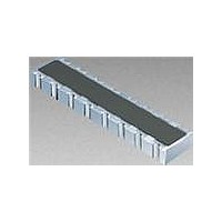
KIT CAY16-J4-LAB2 Bourns Inc., KIT CAY16-J4-LAB2 Datasheet - Page 3

KIT CAY16-J4-LAB2
Manufacturer Part Number
KIT CAY16-J4-LAB2
Description
Resistor Kits CAY16 KIT
Manufacturer
Bourns Inc.
Series
CAY16r
Datasheet
1.KIT_CAY16-J4-LAB2.pdf
(3 pages)
Specifications of KIT CAY16-J4-LAB2
Tolerance
5 %
Power Rating
0.0625 Watt (1/16 Watt)
Package / Case
1205
Termination Style
SMD/SMT
Product
Resistor Networks & Arrays Kit
Operating Temperature Range
- 55 C to + 125 C
Lead Free Status / Rohs Status
Lead free / RoHS Compliant
Specifications are subject to change without notice.
Recommended land pattern design for the chip arrays shown in the following illustration.
A recommended cleaning method is shown in the following table.
1. Land Pattern Design
2. Component Placement
3. Soldering
4. Cleaning
Solvents
Isopropyl alcohol
f
a. Reduce the mechanical stress to a minimum during and after placing of the unit in order not to damage the terminals and
b. Misplacement of components may cause solder bridges.
a. Reflow soldering: Recommendation is shown in the following chart.
b. Wave soldering: Recommendation according to IEC standards.
c. Hand soldering: Don’t touch the protective coating of the part. Solder within 3 seconds when the temperature is over 280ºC.
250
200
150
100
a
Chip Resistor Arrays - Application Note
50
CAY16..4
CAT16..4
protective coating.
0
Model
b
Preheating
60 sec. min.
5 minutes maximum
(.028 to .035)
(.028 to .035)
p
0.7 to 0.9
0.7 to 0.9
Dipping
a
10-30 sec.
Soldering
Cleaning Condition
Solder resist
Land
Chip resistor array CAT
(.016 to .0178)
(.016 to .0178)
0.4 to 0.45
0.4 to 0.45
Gradual Cooling
Ultrasonic Wave Washing
Frequency: 10 to 100kHz
b
1 minute maximum
Power: 20W/L
120 sec. min.
f
a
(.032)
(.032)
0.80
0.80
p
b
(.079 to .087)
(.094 to .11)
2.0 to 2.2
2.4 to 2.8
p
f
DIMENSIONS ARE:
Solder resist
Land
Chip resistor array CAY
(INCHES)
METRIC


