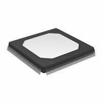
ADSP-21062KS-133 Analog Devices Inc, ADSP-21062KS-133 Datasheet - Page 46

ADSP-21062KS-133
Manufacturer Part Number
ADSP-21062KS-133
Description
IC DSP CONTROLLER 32BIT 240MQFP
Manufacturer
Analog Devices Inc
Series
SHARC®r
Type
Floating Pointr
Specifications of ADSP-21062KS-133
Rohs Status
RoHS non-compliant
Interface
Host Interface, Link Port, Serial Port
Clock Rate
33MHz
Non-volatile Memory
External
On-chip Ram
256kB
Voltage - I/o
5.00V
Voltage - Core
5.00V
Operating Temperature
0°C ~ 85°C
Mounting Type
Surface Mount
Package / Case
240-MQFP, 240-PQFP
Frequency
33MHz
Supply Voltage
5V
Embedded Interface Type
HPI, Serial
No. Of Mips
40
Supply Voltage Range
4.75V To 5.25V
Operating Temperature Range
0°C To +85°C
Device Core Size
32b
Architecture
Super Harvard
Format
Floating Point
Clock Freq (max)
33MHz
Mips
33
Device Input Clock Speed
33MHz
Ram Size
256KB
Program Memory Size
Not RequiredKB
Operating Supply Voltage (typ)
5V
Operating Supply Voltage (min)
4.75V
Operating Supply Voltage (max)
5.25V
Operating Temp Range
0C to 85C
Operating Temperature Classification
Commercial
Mounting
Surface Mount
Pin Count
240
Package Type
MQFP
Lead Free Status / Rohs Status
Not Compliant
Available stocks
Company
Part Number
Manufacturer
Quantity
Price
Company:
Part Number:
ADSP-21062KS-133
Manufacturer:
Analog Devices Inc
Quantity:
10 000
ADSP-21060/ADSP-21060L/ADSP-21062/ADSP-21062L/ADSP-21060C/ADSP-21060LC
JTAG Test Access Port and Emulation
For JTAG Test Access Port and Emulation, see
Figure
Table 36. JTAG Test Access Port and Emulation
1
2
3
Parameter
Timing Requirements
t
t
t
t
t
t
Switching Characteristics
t
t
System Inputs = DATA63–0, ADDR31–0, RD, WR, ACK, SBTS, HBR, HBG, CS, DMAR1, DMAR2, BR6–1, ID2–0, RPBA, IRQ2–0, FLAG3–0, PA, BRST, DR0, DR1, TCLK0,
For ADSP-21060L/ADSP-21060LC/ADSP-21062L, specification is 18.5 ns min.
System Outputs = DATA63–0, ADDR31–0, MS3–0, RD, WR, ACK, PAGE, CLKOUT, HBG, REDY, DMAG1, DMAG2, BR6–1, PA, BRST, CIF, FLAG3–0, TIMEXP, DT0,
TCK
STAP
HTAP
SSYS
HSYS
TRSTW
DTDO
DSYS
TCLK1, RCLK0, RCLK1, TFS0, TFS1, RFS0, RFS1, LxDAT7–0, LxCLK, LxACK, EBOOT, LBOOT, BMS, CLKIN, RESET.
DT1, TCLK0, TCLK1, RCLK0, RCLK1, TFS0, TFS1, RFS0, RFS1, LxDAT7–0, LxCLK, LxACK, BMS.
27.
TCK
TMS
TDI
TDO
SYSTEM
INPUTS
SYSTEM
OUTPUTS
TCK Period
TDI, TMS Setup Before TCK High
TDI, TMS Hold After TCK High
System Inputs Setup Before TCK Low
System Inputs Hold After TCK Low
TRST Pulse Width
TDO Delay from TCK Low
System Outputs Delay After TCK Low
t
DTDO
Figure 27. JTAG Test Access Port and Emulation
Table 36
Rev. F | Page 46 of 64 | March 2008
t
TCK
1, 2
t
t
DSYS
STAP
and
1
3
t
HTAP
t
SSYS
Min
t
5
6
7
18
4t
CK
CK
t
HSYS
Max
13
18.5
Unit
ns
ns
ns
ns
ns
ns
ns
ns


