0W344-004-XTP ON Semiconductor, 0W344-004-XTP Datasheet - Page 8
0W344-004-XTP
Manufacturer Part Number
0W344-004-XTP
Description
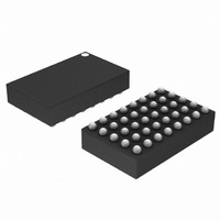
DSP BELASIGNA 200 AUDIO 52-NQFN
Manufacturer
ON Semiconductor
Series
BelaSigna® 200r
Type
Fixed Pointr
Datasheet
1.0W344-005-XTP.pdf
(43 pages)
Specifications of 0W344-004-XTP
Interface
I²C, I²S, PCM, SPI, UART
Clock Rate
33MHz
On-chip Ram
42kB
Operating Temperature
-40°C ~ 85°C
Mounting Type
Surface Mount
Package / Case
52-TFQFN
Lead Free Status / RoHS Status
Lead free / RoHS Compliant
Non-volatile Memory
-
Voltage - I/o
-
Voltage - Core
-
Available stocks
Company
Part Number
Manufacturer
Quantity
Price
Company:

Part Number:
0W344-004-XTP
Manufacturer:
ON Semiconductor
Quantity:
493


BelaSigna 200
4.1.2. QFN Pad Out
Pad #
1
2
3
4
5
6
7
8
9
10
11
12
13
Pad #
14
15
16
17
18
19
20
21
22
23
24
25
26
Pad #
27
28
29
30
31
32
33
34
35
36
37
38
39
Pad #
40
41
42
43
44
45
46
47
48
49
50
51
52
Pad Name
CAP0
VDBL
A|0
A|1/LOUT
A|R
A|2
A|3
VREG
AGND
AI_RC
AOR
AO1/RCVR1-
AO0/RCVR1+
Pad Name
VBAT
RCVR0-
RCVR0+
RCVRGND
GPIO[3]/
NCLK_DIV_RESET/I2S_FA
GPIO[2]/I2S_INA
GPIO[1]/I2S_IND
GPIO[0]/I2S_FD
VDDO
GNDO
EXT_CLK
DEBUG_RX
DEBUG_TX
Pad Name
RESERVED
TWSS_SDA
TWSS_CLK
GNDC
VDDC
SPI_SERO
SPI_SERI
SPI_CS
SPI_CLK
GPIO[15]
GPIO[14]/PCM_FRAME
GPIO[13]/PCM_OUT
GPIO[12]/PCM_IN
Pad Name
N/C
N/C
GPIO[11]/PCM_CLK
GNDO
VDDO
GPIO[10]/DCLK
LSAD[5]/GPIO[9]/UART_RX
LSAD[4]/GPIO[8]/UART_TX
LSAD[3]/GPIO[7]
LSAD[2]/GPIO[6]
LSAD[1]/GPIO[5]/I2S_OUTA
LSAD[0]/GPIO[4]/I2S_OUTD
CAP1
Pad Function
Charge pump capacitor pin 0
Double voltage
Audio signal input to ADC0
Audio signal input to ADC0/line level output signal from preamp 0
Reference voltage for microphone
Audio signal input to ADC1
Audio signal input to ADC1
Regulated voltage for microphone bias
Analog ground
Remote control input
Reference voltage for DAC
Audio signal output from DAC1/output from direct digital drive 1-
Audio signal output from DAC0/output from direct digital drive 1+
Pad Function
TWSS data
TWSS clock
Core logic ground
Core logic, EEPROM and pad supply output
Serial peripheral interface serial data out
Serial peripheral interface serial data in
Serial peripheral interface chip select
Serial peripheral interface clock
General-purpose I/O
General-purpose I/O/PCM interface frame
General-purpose I/O/PCM interface output
General-purpose I/O/PCM interface input
Pad Function
Positive power supply
Output from direct digital drive 0
Output from direct digital drive 0
Receiver return current
General-purpose I/O/clock divider reset/I2S interface
analog blocks frame output
General-purpose I/O/I2S interface analog blocks input
General-purpose I/O/I2S interface analog blocks input
General-purpose I/O/I2S interface digital blocks frame
Digital pads supply input
Digital pads ground
External clock input/internal clock output
Debug port receive
Debut port transmit
Pad Function
No connection
No connection
General-purpose I/O/PCM interface clock
Digital pads ground
Digital pads supply input
General-purpose I/O/class D receiver clock
Low-speed A/D/general-purpose I/O/general-purpose
UART receive
Low-speed A/D input/general-purpose I/O/general-
purpose UART transmit
Low-speed A/D input/general purpose I/P
Low-speed A/D input/general purpose I/P
Low-speed A/D inputs/general-purpose I/O/I2S interface
analog blocks output
Low-speed A/D inputs/general-purpose I/O/I2S interface
analog blocks output
Charge pump capacitor pin 1
Rev. 16 | Page 8 of 43 | www.onsemi.com
N/A
N/A
N/A
N/A
I/O
N/A
N/A
N/A
N/A
I/O
I/O
I/O
N/A
N/A
N/A
N/A
I/O
I/O
I/O
I/O
I/O
I/O
I/O
I/O
I/O
I/O
I/O
I/O
I/O
I/O
I/O
I/O
I/O
I/O
I/O
I/O
I/O
I/O
O
O
O
O
O
O
O
O
I
I
I
I
I
I
I
I
I
I
U/D
U/D
U/D
U/D
N/A
N/A
N/A
N/A
N/A
N/A
N/A
N/A
N/A
N/A
N/A
N/A
N/A
N/A
N/A
N/A
N/A
N/A
N/A
N/A
N/A
N/A
N/A
N/A
N/A
N/A
N/A
N/A
U
U
U
U
U
U
U
U
U
U
U
D
U
D
U
U
U
U
U
U
U
U
U
U
Related parts for 0W344-004-XTP
Image
Part Number
Description
Manufacturer
Datasheet
Request
R

Part Number:
Description:
DSP BELASIGNA 200 AUDIO 52-NQFN
Manufacturer:
ON Semiconductor
Datasheet:

Part Number:
Description:
ON Semiconductor [VOLTAGE REGULATOR]
Manufacturer:
ON Semiconductor
Datasheet:
Part Number:
Description:
357-036-542-201 CARDEDGE 36POS DL .156 BLK LOPRO
Manufacturer:
ON Semiconductor
Datasheet:
Part Number:
Description:
357-036-542-201 CARDEDGE 36POS DL .156 BLK LOPRO
Manufacturer:
ON Semiconductor
Datasheet:
Part Number:
Description:
357-036-542-201 CARDEDGE 36POS DL .156 BLK LOPRO
Manufacturer:
ON Semiconductor
Datasheet:
Part Number:
Description:
357-036-542-201 CARDEDGE 36POS DL .156 BLK LOPRO
Manufacturer:
ON Semiconductor
Datasheet:
Part Number:
Description:
357-036-542-201 CARDEDGE 36POS DL .156 BLK LOPRO
Manufacturer:
ON Semiconductor
Datasheet:
Part Number:
Description:
357-036-542-201 CARDEDGE 36POS DL .156 BLK LOPRO
Manufacturer:
ON Semiconductor
Datasheet:
Part Number:
Description:
357-036-542-201 CARDEDGE 36POS DL .156 BLK LOPRO
Manufacturer:
ON Semiconductor
Datasheet:
Part Number:
Description:
357-036-542-201 CARDEDGE 36POS DL .156 BLK LOPRO
Manufacturer:
ON Semiconductor
Datasheet:
Part Number:
Description:
357-036-542-201 CARDEDGE 36POS DL .156 BLK LOPRO
Manufacturer:
ON Semiconductor
Datasheet:
Part Number:
Description:
357-036-542-201 CARDEDGE 36POS DL .156 BLK LOPRO
Manufacturer:
ON Semiconductor
Datasheet:
Part Number:
Description:
Manufacturer:
ON Semiconductor
Datasheet:
Part Number:
Description:
Manufacturer:
ON Semiconductor
Datasheet: