0W633-001-XTP ON Semiconductor, 0W633-001-XTP Datasheet
0W633-001-XTP
Specifications of 0W633-001-XTP
Available stocks


Related parts for 0W633-001-XTP

0W633-001-XTP Summary of contents
Page 1
... January, 2011 − Rev. 8 http://onsemi.com CABGA−57 PLASTIC CASE 566AA MARKING DIAGRAMS XXXXYZZ BELASIGNA 250 0W888−002 AAAA 0W888−002 = 64 LFBGA Option 0W633 = 57 CABGA Option XXXX = Date Code Y = Assembly Plant Identifier ZZ = Traceability Code AAAA = Country of Assembly BELASIGNA250 48−06−G XXXXYZZ ...
Page 2
Contents Introduction . . . . . . . . . . . . . . . . . . . . . . . . . . . . . . . . . . . . . . ...
Page 3
Electrical Performance Specifications The parameters in Table 2 do not vary with WOLA filterbank configuration. The tests were performed at 20°C with a clean 1.8 V supply voltage. BelaSigna 250 was running in high voltage mode (VDDC = 1.8 V). ...
Page 4
Table 2. ELECTRICAL SPECIFICATIONS Description Symbol POWER−ON−RESET (POR) POR hysteresis POR HYSTERESIS POR duration INPUT STAGE Analog input voltage Preamplifier gain tolerance Preamplifier gain mismatch between channels Input impedance Input referred noise Input dynamic range Input peak THD+N (Note 4) ...
Page 5
Table 2. ELECTRICAL SPECIFICATIONS Description Symbol ANALOG OUTPUT STAGE Attenuator gain tolerance Output impedance Output noise OUT Output dynamic range OUT Output THD+N OUT ANTI−ALIASING FILTERS (Input and Output) Preamplifier filter cut−off frequency Digital anti−aliasing filter cut−off frequency Analog output ...
Page 6
Table 2. ELECTRICAL SPECIFICATIONS Description Symbol OSCILLATION CIRCUITRY Internal oscillator frequency SYS_CLK Calibrated clock frequency SYS_CLK Internal oscillator jitter External oscillator tolerances Maximum working frequency CLK IR INTERFACE Carrier frequency Data rate Input current DIGITAL INTERFACES TWSS baud rate General−purpose ...
Page 7
... A separate data sheet is available for this part (part number 0W548−001−XTD). Contact ON Semiconductor for more information on this package option. All BelaSigna 250 package options are Green (RoHS− compliant). Contact ON Semiconductor for supporting documentation. Description Power supply Analog ground ...
Page 8
Table 3. LFBGA PIN DESCRIPTIONS Pad Index BelaSigna 250 Pin Name A4 SPI_SERI E6 TWSS_CLK F8 TWSS_DATA G5 GPIO[0] / I2S_FD H5 GPIO[1] / I2S_IND G4 GPIO[2] / I2S_INA F5 GPIO[3] / NCLK_DIV_RESET / I2S_FA B5 GPIO[4] / LSAD [0] ...
Page 9
Table 4. CABGA PIN DESCRIPTIONS Pad Index BelaSigna 250 Pad Name H1 CAP0 G1 CAP1 J2 AI0 H3 AI1/LOUT J4 AI2 H4 AI3 J3 AIR G9 RCVR0+ H9 RCVR0− J9 AO0/RCVR1+ J8 AO1/RCVR1− J7 AOR B9 DEBUG_RX A9 DEBUG_TX C9 ...
Page 10
A total of 48 active pins are present on this WLCSP package of BelaSigna 250. A description of these pads is given in Table 5. Table 5. WLCSP PIN DESCRIPTIONS Pad Index BelaSigna 250 Pad Name D4 VBAT D3, C3 ...
Page 11
... ON Semiconductor can provide BelaSigna 250 WLCSP land pattern CAD files to assist your PCB design upon request. Recommended Ground Design Strategy The ground plane should be partitioned into two: the analog ground plane (AGND) and the digital ground plane (DGND) ...
Page 12
R GNDD U8 GPIO15 GPIO[15] GPIO14 GPIO[14]/PCM_FRAME/REMOTE GPIO13 GPIO[13]/PCM_SERO GPIO12 GPIO[12]/PCM_SERI GPIO11 GPIO[11]/PCM_CLK GPIO10 GPIO[10]/UCLK GPIO9 LSAD[5]/GPIO[9]/UART_RX GPIO8 LSAD[4]/GPIO[8]/UART_TX GPIO7 LSAD[3]/GPIO[7] GPIO6 LSAD[2]/GPIO[6] GPIO5 LSAD[1]/GPIO[5]/I2S_OUTA GPIO4 LSAD[0]/GPIO[4]/I2S_OUTD GPIO3 GPIO[3]/NCLK_DIV_RESET/I2S_FA GPIO2 GPIO[2]/I2S_INA GPIO1 GPIO[1]/I2S_IND GPIO0 GPIO[0]/I2S_FD VDBL VREG ...
Page 13
Internal Power Supplies Power management circuitry in BelaSigna 250 generates separate digital (VDDC) and analog (VREG, VDBL) regulated supplies. Each supply requires an external decoupling capacitor, even if the supply is not used externally. Decoupling capacitors should be placed as ...
Page 14
Audio Inputs The audio input traces should be as short as possible. The input impedance of each audio input pad (e.g., AI0, AI1, etc.,) is high (approximately 500 kW); therefore capacitor is sufficient to decouple the DC ...
Page 15
X Y Multiplier PH PL ALU Barrel Shifter Limiter Internal Routing The RCore is a single−cycle pipelined multiply− accumulate (MAC) architecture that feeds into a 40−bit accumulator complete with barrel shifter for fast normalization and de−normalization operations. ...
Page 16
Table 8. INSTRUCTION SET Instruction Description ABS A [,Cond] [,DW] Calculate absolute value condition ADD A, Reg [,C] Add register to A ADD A, (Rij) [,C] Add memory to A ADD A, DRAM [,B] Add (DRAM) to ...
Page 17
Instruction Description MSET Reg, (Ri) [,SQ] Multiplier load MUL [Cond] [,A] [,P] Update A and/ with X*Y on condition NEG A [,Cond] [,DW] Calculate negative value condition NOP No operation OR A, Reg OR ...
Page 18
Weighted Overlap−Add (WOLA) Filterbank Coprocessor Time−domain input 1. Filterbank Analysis (Length: La) Figure 4. WOLA Filterbank Coprocessor Architecture The WOLA coprocessor performs high−fidelity filterbank processing to provide efficient time−frequency processing and alias−free gain adjustments. The WOLA coprocessor stores intermediate data ...
Page 19
WOLA Coprocessor FIFO * mono Mono Mode WOLA Coprocessor FIFO * stereo Digital Mixed Mode * Real & Complex Gain Application Other Digital Blocks and Functions RAM and ROM There are 20−Kwords of on−chip program and data RAM on BelaSigna ...
Page 20
Memory Maps Complete memory maps for BelaSigna 250 are shown in Figure 6. X:0xFFFF X:0x423F Window (192 x 16) X:0x4180 X:0x417F Gain (256 x 16) X:0x4080 X:0x407F Microcode (128 x 16) X:0x4000 X:0x207F ROM LUT (128 x 16) X:0x2000 X:0x1B7F ...
Page 21
Table 10. INTERRUPT DESCRIPTIONS Interrupt WOLA_DONE WOLA function done IO_BLOCK_FULL IOP interrupt GP_TIMER General−purpose timer interrupt WATCHDOG_TIMER Watchdog timer interrupt SPI_INTERFACE SPI interface interrupt IR IR remote interrupt EXT3_RX EXT3 register receive interrupt EXT3_TX EXT3 register transmit interrupt GPIO User ...
Page 22
Output Stage The analog audio output and the digital output are composed of two individual channels. The first part of the output stage interpolates the signal for highly oversampled D/A conversion and automatically configures itself for the desired over−sampling rate. ...
Page 23
... During the power−on procedure, all audio outputs are muted; all RCore registers and all control registers (analog and digital) are set to default values. (Please contact ON Semiconductor for more information on default values associated with each control register.) BelaSigna 250 boots in a two− ...
Page 24
... POR code. Subsequently, the signal−processing application that is stored in the EEPROM is downloaded to PRAM by the bootloader. The boot process generally takes less than one second. ON Semiconductor provides a standard full−feature bootloader. A graphical representation of this booting sequence can be seen in Figure 9. Program Memory Bootloader ...
Page 25
VDDCnominal VDDCstartup VDDCshutdown Internal Reset Signal Normal Power−Up Other Analog Support Blocks and Functions Multi−Chip Sample Clock (MCLK) Synchronization BelaSigna 250 allows MCLK synchronization between two or more BelaSigna 250 devices connected in a multi−chip configuration. Samples on multiple chips ...
Page 26
... Configurable high−speed RS−232 universal asynchronous receiver/transmitter (UART). Assembly Information Carrier Details LFBGA ON Semiconductor offers tape and reel packing for BelaSigna 250 LFBGA packages. The packing consists of a pocketed carrier tape, a cover tape, and a molded Quantity per Reel: 1500 units Pin 1 Orientation: Upper Left Each complete reel contains 1500 parts ...
Page 27
... CABGA ON Semiconductor offers tape and reel packing for BelaSigna 250 CABGA packages. The packing consists of a pocketed carrier tape, a cover tape, and a molded anti−static polystyrene reel. The carrier and cover tape Quantity per Reel: 5000 units Pin 1 Orientation: Upper Left Each complete reel contains 5000 parts ...
Page 28
... WLCSP ON Semiconductor offers tape and reel packing for BelaSigna 250 WLCSP packages. The packing consists of a pocketed carrier tape, a cover tape, and a molded 1. 10 sprockets hole pitch cumulative tolerance ±0.1. 2. Camber in compliance with EIA 763. 3. Pocket position relative to sprocket hole measured as true position of pocket, not pocket hole. ...
Page 29
... BelaSigna 250. Training To facilitate development on the BelaSigna 250 platform, training is available upon request. Contact your account manager for more information. Company or Product Inquiries For more information about ON Semiconductor products or services visit our Web site at http://onsemi.com. http://onsemi.com 29 ...
Page 30
X D PIN 1 CORNER 0 e e/2 D1 VIEW M−M PACKAGE DIMENSIONS LFBGA 64 BALLS, ...
Page 31
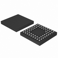
PACKAGE DIMENSIONS CABGA 57, 5x5 CASE 566AA−01 ISSUE A http://onsemi.com 31 ...
Page 32
... 0. BOTTOM VIEW *For additional information on our Pb−Free strategy and soldering details, please download the ON Semiconductor Soldering and Mounting Techniques Reference Manual, SOLDERRM/D. PACKAGE DIMENSIONS WLCSP48, 3.80x2.58 CASE 567AS−01 ISSUE B A PIN A1 REFERENCE È È SEATING C PLANE e e RECOMMENDED ...
Page 33
... Table 12. ORDERING INFORMATION Part Number Package 0W633−001−XTP CABGA 0W888−002−XTP LFBGA B250W48A106XXG 2.6 x 3.8 mm WLCSP BelaSigna is a registered trademark of Semiconductor Components Industries, LLC. ON Semiconductor and are registered trademarks of Semiconductor Components Industries, LLC (SCILLC). SCILLC reserves the right to make changes without further notice to any products herein ...