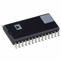
ADMCF327BR Analog Devices Inc, ADMCF327BR Datasheet - Page 14

ADMCF327BR
Manufacturer Part Number
ADMCF327BR
Description
IC DSP SW MOTOR CTRLR 28SOIC
Manufacturer
Analog Devices Inc
Series
Motor Controlr
Type
Fixed Pointr
Datasheet
1.ADMCF327BR.pdf
(36 pages)
Specifications of ADMCF327BR
Rohs Status
RoHS non-compliant
Interface
Synchronous Serial Port (SSP)
Clock Rate
20MHz
Non-volatile Memory
FLASH (12 kB), ROM (12kB)
On-chip Ram
2.5kB
Voltage - I/o
5.00V
Voltage - Core
5.00V
Operating Temperature
-40°C ~ 85°C
Mounting Type
Surface Mount
Package / Case
28-SOIC (7.5mm Width)
Lead Free Status / Rohs Status
Not Compliant
ADMCF327
over half the PWM period. The switching signals produced by
the three-phase timing unit are also adjusted to incorporate the
programmed dead time value in the PWMDT register.
The PWM is center-based. This means that in single update mode
the resulting output waveforms are symmetrical and centered in
the PWMSYNC period. Figure 7 presents a typical PWM tim-
ing diagram illustrating the PWM-related registers’ (PWMCHA,
PWMTM, PWMDT, and PWMSYNCWT) control over the
waveform timing in both half cycles of the PWM period. The
magnitude of each parameter in the timing diagram is determined
by multiplying the integer value in each register by t
50 ns). It may be seen in the timing diagram how dead time is
incorporated into the waveforms by moving the switching edges
away from the instants set by the PWMCHA register.
Each switching edge is moved by an equal amount (PWMDT
× t
pulse, whose width is set by the PWMSYNCWT register, is also
shown. Bit 3 of the SYSSTAT register indicates which half cycle
is active. This can be useful in double update mode, as will be
discussed later.
The resultant on-times of the PWM signals shown in Figure 7
may be written as:
The corresponding duty cycles are:
Obviously, negative values of T
because the minimum permissible value is zero, corresponding
to a 0% duty cycle. In a similar fashion, the maximum value is
T
The output signals from the timing unit for operation in double
update mode are shown in Figure 8. This illustrates a completely
general case where the switching frequency, dead time and duty
cycle are all changed in the second half of the PWM period. Of
course, the same value for any or all of these quantities could be
used in both halves of the PWM cycle. However, it can be seen
that there is no guarantee that symmetrical PWM signals will
be produced by the timing unit in this double update mode.
SYSSTAT (3)
S
PWMSYNC
CK
, corresponding to a 100% duty cycle.
T
T
) to preserve the symmetrical output patterns. The PWMSYNC
AH
AL
d
d
AH
AL
AH
AL
=
=
2
=
2
=
×
2
T
×
T
T
T
AL
(
AH
(
S
S
PWMTM
PWMDT
PWMCHA
=
=
PWMTM
PWMTM
PWMCHA
–
PWMCHA
PWMTM
–
PWMCHA
PWMDT
–
AH
–
PWMCHA
PWMTM
and T
PWMDT
PWMCHA
)
–
AL
×
PWMDT
t
are not permitted
PWMSYNCWT + 1
CK
PWMTM
–
PWMDT
2
CK
PWMDT
)
(typically
×
t
CK
Additionally, it is seen that the dead time is inserted into the
PWM signals in the same way as in the single update mode.
In general, the on-times of the PWM signals in double update
mode are defined by:
where the subscript 1 refers to the value of that register during
the first half cycle and the subscript 2 refers to the value during
the second half cycle. The corresponding duty cycles are:
because for the completely general case in double update mode,
the switching period is given by:
Again, the values of T
zero and T
PWM signals similar to those illustrated in Figure 7 and Figure
8 can be produced on the BH, BL, CH, and CL outputs by pro-
gramming the PWMCHB and PWMCHC registers in a manner
identical to that described for PWMCHA.
The PWM controller does not produce any PWM outputs until
all of the PWMTM, PWMCHA, PWMCHB, and PWMCHC
registers have been written to at least once. After these registers
have been written, the counters in the three-phase timing unit
T
SYSSTAT (3)
T
AH
PWMSYNC
AL
= (PWMCHA
= (PWMTM
AH
d
d
AL
AH
AL
S
.
2
=
=
=
−
=
–
T
T
PWMDT
PWMTM
(
T
PWMCHA
(
S
PWMSYNCWT
T
PWMDT
PWMCHA
T
PWMTM
PWMTM
AL
AH
= (PWMTM
S
PWMDT
S
PWMTM
1
1
+ PWMCHA
+ PWMTM
1
AH
PWMTM
PWMTM
1
and T
PWMCHA
1
1
1
1
1
1
+
+
1
+ 1
2
+
– PWMDT
+
+
PWMDT
PWMTM
+
PWMTM
1
PWMCHA
PWMTM
AL
PWMDT
+ PWMTM
2
1
2
– PWMCHA
1
– PWMDT
1
are constrained to lie between
+
PWMCHA
+
PWMTM
PWMTM
2
2
2
2
) × t
1
2
2
+
+
2
PWMTM
2
PWMCHA
PWMDT
) × t
PWMSYNCWT
1
CK
1
– PWMDT
2
2
– PWMCHA
CK
2
2
PWMDT
2
)
2
1
+ 1
)
2
) × t
2
2
–
CK


