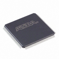
EP2C5T144C6N Altera, EP2C5T144C6N Datasheet - Page 99

EP2C5T144C6N
Manufacturer Part Number
EP2C5T144C6N
Description
IC CYCLONE II FPGA 5K 144-TQFP
Manufacturer
Altera
Series
Cyclone® IIr
Datasheet
1.EP2C5T144C8N.pdf
(168 pages)
Specifications of EP2C5T144C6N
Number Of Logic Elements/cells
4608
Number Of Labs/clbs
288
Total Ram Bits
119808
Number Of I /o
89
Voltage - Supply
1.15 V ~ 1.25 V
Mounting Type
Surface Mount
Operating Temperature
0°C ~ 85°C
Package / Case
144-TQFP, 144-VQFP
Family Name
Cyclone® II
Number Of Logic Blocks/elements
4608
# I/os (max)
89
Frequency (max)
500MHz
Process Technology
90nm
Operating Supply Voltage (typ)
1.2V
Logic Cells
4608
Ram Bits
119808
Operating Supply Voltage (min)
1.15V
Operating Supply Voltage (max)
1.25V
Operating Temp Range
0C to 85C
Operating Temperature Classification
Commercial
Mounting
Surface Mount
Pin Count
144
Package Type
TQFP
Lead Free Status / RoHS Status
Lead free / RoHS Compliant
Number Of Gates
-
Lead Free Status / Rohs Status
Compliant
Other names
544-2137
Available stocks
Company
Part Number
Manufacturer
Quantity
Price
Company:
Part Number:
EP2C5T144C6N
Manufacturer:
ALTERA
Quantity:
5
Part Number:
EP2C5T144C6N
Manufacturer:
ALTERA/阿尔特拉
Quantity:
20 000
Altera Corporation
February 2008
Notes to
(1)
(2)
(3)
(4)
(5)
(6)
LVDS
Mini-LVDS
(2)
RSDS
LVPECL
(3) (6)
Differential
1.5-V HSTL
class I
and II
Differential
1.8-V HSTL
class I
and II
Differential
SSTL-2
class I
and II
Differential
SSTL-18
class I
and II
Table 5–8. Recommended Operating Conditions for User I/O Pins Using Differential Signal I/O Standards
Standard
I/O
Refer to the
measurement conditions on V
The RSDS and mini-LVDS I/O standards are only supported on output pins.
The LVPECL I/O standard is only supported on clock input pins. This I/O standard is not supported on output
pins.
The differential 1.8-V and 1.5-V HSTL I/O standards are only supported on clock input pins and PLL output clock
pins.
The differential SSTL-18 and SSTL-2 I/O standards are only supported on clock input pins and PLL output clock
pins.
The LVPECL clock inputs are powered by V
connect V
(4)
(4)
(5)
(5)
(2)
Table
2.375
2.375
2.375
3.135
1.425
2.375
CCIO
1.71
Min
5–8:
1.7
High-Speed Differential Interfaces in Cyclone II Devices
to typical value of 3.3V.
V
CCIO
Typ
2.5
2.5
2.5
3.3
1.5
1.8
2.5
1.8
(V)
2.625
2.625
2.625
3.465
1.575
2.625 0.36
Max
1.89
1.9
Table 5–8
pins with differential I/O standards.
ID
.
0.25
Min
0.1
0.1
0.2
—
—
—
V
shows the recommended operating conditions for user I/O
ID
Typ
0.6
—
—
—
—
—
—
—
(V)
CCINT
(1)
V
V
V
+ 0.6
+ 0.6
+ 0.6
Max
0.65
0.95
C C I O
C C I O
C C I O
—
—
—
and support all V
V
V
0.5 ×
– 0.2
0.5 ×
– 0.2
0.68
Min
C C I O
C C I O
0.1
—
—
—
—
DC Characteristics and Timing Specifications
chapter of the Cyclone II Device Handbook for
V
V
V
ICM
0.5 ×
0.5 ×
Typ
C C I O
C C I O
CCIO
—
—
—
—
—
—
Cyclone II Device Handbook, Volume 1
(V)
settings. However, it is recommended to
V
V
0.5 ×
+ 0.2
0.5 ×
+ 0.2
Max
C C I O
C C I O
2.0
0.9
—
—
—
—
Min
—
—
—
—
—
—
—
0
V
IL
(V)
– 0.20
– 0.20
– 0.35
– 0.25
V
V
V
V
Max
2.2
R E F
R E F
R E F
R E F
—
—
—
+ 0.20
+ 0.20
+ 0.35
+ 0.25
V
V
V
V
Min
2.1
—
—
—
R E F
R E F
R E F
R E F
V
IH
(V)
2.88
Max
—
—
—
—
—
—
—
5–9


