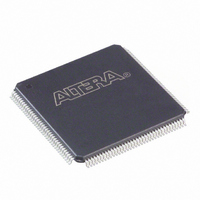
EP1K30TC144-2 Altera, EP1K30TC144-2 Datasheet - Page 16

EP1K30TC144-2
Manufacturer Part Number
EP1K30TC144-2
Description
IC ACEX 1K FPGA 30K 144-TQFP
Manufacturer
Altera
Series
ACEX-1K®r
Datasheet
1.EP1K10TC100-3N.pdf
(86 pages)
Specifications of EP1K30TC144-2
Number Of Logic Elements/cells
1728
Number Of Labs/clbs
216
Total Ram Bits
24576
Number Of I /o
102
Number Of Gates
119000
Voltage - Supply
2.375 V ~ 2.625 V
Mounting Type
Surface Mount
Operating Temperature
0°C ~ 70°C
Package / Case
144-TQFP, 144-VQFP
Family Name
ACEX™ 1K
Number Of Usable Gates
30000
Number Of Logic Blocks/elements
1728
# I/os (max)
102
Frequency (max)
200MHz
Process Technology
CMOS
Operating Supply Voltage (typ)
2.5V
Logic Cells
1728
Ram Bits
24576
Device System Gates
119000
Operating Supply Voltage (min)
2.375V
Operating Supply Voltage (max)
2.625V
Operating Temp Range
0C to 70C
Operating Temperature Classification
Commercial
Mounting
Surface Mount
Pin Count
144
Package Type
TQFP
Lead Free Status / RoHS Status
Contains lead / RoHS non-compliant
Other names
544-1066
Available stocks
Company
Part Number
Manufacturer
Quantity
Price
Company:
Part Number:
EP1K30TC144-2
Manufacturer:
ALTERA
Quantity:
1 831
Company:
Part Number:
EP1K30TC144-2
Manufacturer:
ALTERA
Quantity:
155
Part Number:
EP1K30TC144-2
Manufacturer:
ALTERA/阿尔特拉
Quantity:
20 000
Company:
Part Number:
EP1K30TC144-2N
Manufacturer:
ALTERA
Quantity:
1 500
Company:
Part Number:
EP1K30TC144-2N
Manufacturer:
ALTERA
Quantity:
5 510
ACEX 1K Programmable Logic Device Family Data Sheet
Figure 8. ACEX 1K Logic Element
16
Chip-Wide
labctrl1
labctrl2
labctrl3
labctrl4
data1
data2
data3
data4
Reset
Look-Up
The programmable flipflop in the LE can be configured for D, T, JK, or SR
operation. The clock, clear, and preset control signals on the flipflop can
be driven by global signals, general-purpose I/O pins, or any internal
logic. For combinatorial functions, the flipflop is bypassed and the LUT’s
output drives the LE’s output.
The LE has two outputs that drive the interconnect: one drives the local
interconnect, and the other drives either the row or column FastTrack
Interconnect routing structure. The two outputs can be controlled
independently. For example, the LUT can drive one output while the
register drives the other output. This feature, called register packing, can
improve LE utilization because the register and the LUT can be used for
unrelated functions.
The ACEX 1K architecture provides two types of dedicated high-speed
data paths that connect adjacent LEs without using local interconnect
paths: carry chains and cascade chains. The carry chain supports high-
speed counters and adders, and the cascade chain implements wide-input
functions with minimum delay. Carry and cascade chains connect all LEs
in a LAB and all LABs in the same row. Intensive use of carry and cascade
chains can reduce routing flexibility. Therefore, the use of these chains
should be limited to speed-critical portions of a design.
Preset
Clear/
Logic
Select
Clock
(LUT)
Table
Carry-Out
Carry-In
Chain
Carry
Cascade-Out
Cascade-In
Cascade
Chain
Register Bypass
D
ENA
CLRN
PRN
Q
Altera Corporation
Programmable
Register
To FastTrack
Interconnect
To LAB Local
Interconnect


