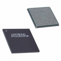
EP1C20F400C6 Altera, EP1C20F400C6 Datasheet - Page 32

EP1C20F400C6
Manufacturer Part Number
EP1C20F400C6
Description
IC CYCLONE FPGA 20K LE 400-FBGA
Manufacturer
Altera
Series
Cyclone®r
Datasheet
1.EP1C3T144C8.pdf
(106 pages)
Specifications of EP1C20F400C6
Number Of Logic Elements/cells
20060
Number Of Labs/clbs
2006
Total Ram Bits
294912
Number Of I /o
301
Voltage - Supply
1.425 V ~ 1.575 V
Mounting Type
Surface Mount
Operating Temperature
0°C ~ 85°C
Package / Case
400-FBGA
Family Name
Cyclone®
Number Of Logic Blocks/elements
20060
# I/os (max)
301
Frequency (max)
405.2MHz
Process Technology
0.13um (CMOS)
Operating Supply Voltage (typ)
1.5V
Logic Cells
20060
Ram Bits
294912
Operating Supply Voltage (min)
1.425V
Operating Supply Voltage (max)
1.575V
Operating Temp Range
0C to 85C
Operating Temperature Classification
Commercial
Mounting
Surface Mount
Pin Count
400
Package Type
FBGA
Lead Free Status / RoHS Status
Contains lead / RoHS non-compliant
Number Of Gates
-
Lead Free Status / Rohs Status
Not Compliant
Other names
544-1046
Available stocks
Company
Part Number
Manufacturer
Quantity
Price
Company:
Part Number:
EP1C20F400C6
Manufacturer:
ALTERA
Quantity:
2
Company:
Part Number:
EP1C20F400C6
Manufacturer:
MAXIM
Quantity:
10
Company:
Part Number:
EP1C20F400C6
Manufacturer:
ALTERA
Quantity:
3 000
Part Number:
EP1C20F400C6
Manufacturer:
ALTERA/阿尔特拉
Quantity:
20 000
Company:
Part Number:
EP1C20F400C6AB
Manufacturer:
ALTERA
Quantity:
3 000
Company:
Part Number:
EP1C20F400C6N
Manufacturer:
ALTERA
Quantity:
237
Cyclone Device Handbook, Volume 1
Figure 2–18. Input/Output Clock Mode in True Dual-Port Mode
Notes to
(1)
(2)
2–26
Preliminary
clken
clock
wren
A
A
A
data
byteena
address
All registers shown have asynchronous clear ports.
Violating the setup or hold time on the address registers could corrupt the memory contents. This applies to both
read and write operations.
A
[ ]
6
A
A
[ ]
Figure
[ ]
6 LAB Row Clocks
2–18:
D
ENA
D
ENA
D
ENA
D
ENA
Q
Q
Q
Q
Generator
Pulse
Write
D
ENA
Data In
Byte Enable A
Address A
Write/Read
Enable
Data Out
Q
A
Memory Block
256 × 16 (2)
q
1,024 × 4
2,048 × 2
4,096 × 1
A
512 × 8
[ ]
q
B
[ ]
Byte Enable B
Write/Read
Address B
Data Out
B
Data In
Enable
Q
ENA
D
Notes
Generator
Write
Pulse
(1),
(2)
Q
Q
Q
Q
ENA
ENA
ENA
ENA
D
D
D
D
Altera Corporation
May 2008
6
data
byteena
address
wren
clken
clock
B
B
B
B
[ ]
B
B
[ ]
[ ]


