EP2C35F672C6 Altera, EP2C35F672C6 Datasheet - Page 152
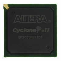
EP2C35F672C6
Manufacturer Part Number
EP2C35F672C6
Description
IC CYCLONE II FPGA 33K 672-FBGA
Manufacturer
Altera
Series
Cyclone® IIr
Datasheet
1.EP2C5T144C8N.pdf
(168 pages)
Specifications of EP2C35F672C6
Number Of Logic Elements/cells
33216
Number Of Labs/clbs
2076
Total Ram Bits
483840
Number Of I /o
475
Voltage - Supply
1.15 V ~ 1.25 V
Mounting Type
Surface Mount
Operating Temperature
0°C ~ 85°C
Package / Case
672-FBGA
Family Name
Cyclone® II
Number Of Logic Blocks/elements
33216
# I/os (max)
475
Frequency (max)
500MHz
Process Technology
90nm
Operating Supply Voltage (typ)
1.2V
Logic Cells
33216
Ram Bits
483840
Operating Supply Voltage (min)
1.15V
Operating Supply Voltage (max)
1.25V
Operating Temp Range
0C to 85C
Operating Temperature Classification
Commercial
Mounting
Surface Mount
Pin Count
672
Package Type
FBGA
For Use With
P0301 - DE2 CALL FOR ACADEMIC PRICING544-1733 - PCI KIT W/CYCLONE II EP2C35N649-1001 - KIT DEV CYCLONE II PCI EXPRESS
Lead Free Status / RoHS Status
Contains lead / RoHS non-compliant
Number Of Gates
-
Lead Free Status / Rohs Status
Not Compliant
Other names
544-1087
EP2C35F672C6ES
EP2C35F672C6ES
Available stocks
Company
Part Number
Manufacturer
Quantity
Price

Company:
Part Number:
EP2C35F672C6N
Manufacturer:
ALTERA
Quantity:
170


Timing Specifications
5–62
Cyclone II Device Handbook, Volume 1
Notes to
(1)
(2)
(3)
(4)
(5)
(6)
(7)
(8)
(9)
(10) For extended temperature devices, the maximum output jitter (peak to peak) is 600 ps.
(11) For extended temperature devices, the maximum t
(12) For extended temperature devices, the maximum lock time is 500 us.
t
t
F A L L
L O C K
Table 5–50. LVDS Transmitter Timing Specification (Part 2 of 2)
Symbol
The maximum data rate that complies with duty cycle distortion of 45–55%.
The maximum data rate when taking duty cycle in absolute ps into consideration that may not comply with 45–55%
duty cycle distortion. If the downstream receiver can handle duty cycle distortion beyond the 45–55% range, you
may use the higher data rate values from this column. You can calculate the duty cycle distortion as a percentage
using the absolute ps value. For example, for a data rate of 640 Mbps (UI = 1562.5 ps) and a t
duty cycle distortion is ± t
distortion of 42–58%.
The TCCS specification applies to the entire bank of LVDS, as long as the SERDES logic is placed within the LAB
adjacent to the output pins.
For extended temperature devices, the maximum input clock frequency for ×10 through ×2 modes is 137.5 MHz.
For extended temperature devices, the maximum data rate for ×10 through ×2 modes is 275 Mbps.
For extended temperature devices, the maximum input clock frequency for ×10 through ×2 modes is 200 MHz.
For extended temperature devices, the maximum data rate for ×10 through ×2 modes is 400 Mbps.
For extended temperature devices, the maximum input clock frequency for ×1 mode is 340 MHz.
For extended temperature devices, the maximum data rate for ×1 mode is 340 Mbps.
Table
Conditions
80–20%
—
5–50:
Min
150
—
–6 Speed Grade
D U T Y
Typ
200
—
/(UI*2) *100% = ± 250 ps/(1562.5 *2) * 100% = ± 8%, which gives you a duty cycle
Max
(1)
250
100
Max
(2)
Min
150
—
R I S E
–7 Speed Grade
and t
Typ
200
—
FA L L
Max
(1)
are 300 ps.
250
100
Max
(2)
Min
150
—
–8 Speed Grade
Typ
200
—
Altera Corporation
D U T Y
Max
(1)
250
100
February 2008
of 250 ps, the
(11)
(12)
Max
(2)
Unit
ps
μs
Related parts for EP2C35F672C6
Image
Part Number
Description
Manufacturer
Datasheet
Request
R

Part Number:
Description:
CYCLONE II STARTER KIT EP2C20N
Manufacturer:
Altera
Datasheet:


Part Number:
Description:
CPLD, EP610 Family, ECMOS Process, 300 Gates, 16 Macro Cells, 16 Reg., 16 User I/Os, 5V Supply, 35 Speed Grade, 24DIP
Manufacturer:
Altera Corporation
Datasheet:
Part Number:
Description:
CPLD, EP610 Family, ECMOS Process, 300 Gates, 16 Macro Cells, 16 Reg., 16 User I/Os, 5V Supply, 15 Speed Grade, 24DIP
Manufacturer:
Altera Corporation
Datasheet:
Part Number:
Description:
Manufacturer:
Altera Corporation
Datasheet:
Part Number:
Description:
CPLD, EP610 Family, ECMOS Process, 300 Gates, 16 Macro Cells, 16 Reg., 16 User I/Os, 5V Supply, 30 Speed Grade, 24DIP
Manufacturer:
Altera Corporation
Datasheet:
Part Number:
Description:
High-performance, low-power erasable programmable logic devices with 8 macrocells, 10ns
Manufacturer:
Altera Corporation
Datasheet:
Part Number:
Description:
High-performance, low-power erasable programmable logic devices with 8 macrocells, 7ns
Manufacturer:
Altera Corporation
Datasheet:
Part Number:
Description:
Classic EPLD
Manufacturer:
Altera Corporation
Datasheet:
Part Number:
Description:
High-performance, low-power erasable programmable logic devices with 8 macrocells, 10ns
Manufacturer:
Altera Corporation
Datasheet:
Part Number:
Description:
Manufacturer:
Altera Corporation
Datasheet:
Part Number:
Description:
Manufacturer:
Altera Corporation
Datasheet:
Part Number:
Description:
Manufacturer:
Altera Corporation
Datasheet:
Part Number:
Description:
CPLD, EP610 Family, ECMOS Process, 300 Gates, 16 Macro Cells, 16 Reg., 16 User I/Os, 5V Supply, 25 Speed Grade, 24DIP
Manufacturer:
Altera Corporation
Datasheet: