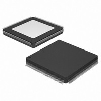
XC3S200-4PQG208C Xilinx Inc, XC3S200-4PQG208C Datasheet - Page 96

XC3S200-4PQG208C
Manufacturer Part Number
XC3S200-4PQG208C
Description
IC SPARTAN-3 FPGA 200K 208-PQFP
Manufacturer
Xilinx Inc
Series
Spartan™-3r
Datasheet
1.XC3S50-4VQG100C.pdf
(217 pages)
Specifications of XC3S200-4PQG208C
Total Ram Bits
221184
Number Of Logic Elements/cells
4320
Number Of Labs/clbs
480
Number Of I /o
141
Number Of Gates
200000
Voltage - Supply
1.14 V ~ 1.26 V
Mounting Type
Surface Mount
Operating Temperature
0°C ~ 85°C
Package / Case
208-BFQFP
No. Of Logic Blocks
480
No. Of Gates
200000
No. Of Macrocells
4320
Family Type
Spartan-3
No. Of Speed Grades
4
No. Of I/o's
141
Clock
RoHS Compliant
Lead Free Status / RoHS Status
Lead free / RoHS Compliant
Other names
122-1339
Available stocks
Company
Part Number
Manufacturer
Quantity
Price
Company:
Part Number:
XC3S200-4PQG208C
Manufacturer:
XILINX/42
Quantity:
1 640
Part Number:
XC3S200-4PQG208C
Manufacturer:
XILINX/赛灵思
Quantity:
20 000
- Current page: 96 of 217
- Download datasheet (6Mb)
Spartan-3 FPGA Family: DC and Switching Characteristics
Table 67: Timing for the JTAG Test Access Port
96
Notes:
1.
Clock-to-Output Times
T
Setup Times
T
T
Hold Times
T
T
Clock Timing
T
T
F
TCKTDO
TDITCK
TMSTCK
TCKTDI
TCKTMS
TCKH
TCKL
TCK
The numbers in this table are based on the operating conditions set forth in
Symbol
TCK
TMS
TDI
TDO
(Input)
(Input)
(Input)
(Output)
The time from the falling transition on the TCK pin to data
appearing at the TDO pin
The time from the setup of data at the TDI pin to the rising
transition at the TCK pin
The time from the setup of a logic level at the TMS pin to the
rising transition at the TCK pin
The time from the rising transition at the TCK pin to the point
when data is last held at the TDI pin
The time from the rising transition at the TCK pin to the point
when a logic level is last held at the TMS pin
TCK pin High pulse width
TCK pin Low pulse width
Frequency of the TCK signal
T
TDITCK
T
TMSTCK
Figure 37: JTAG Waveforms
Description
www.xilinx.com
T
TCKTDI
T
TCKTMS
JTAG Configuration
Boundary-Scan
Table
T
TCKTDO
31.
T
CCH
All Speed Grades
1/F
Min
1.0
7.0
7.0
DS099-3 (v2.5) December 4, 2009
0
0
5
5
0
0
TCK
T
CCL
Product Specification
Max
11.0
DS099_06_102909
33
25
∞
∞
-
-
-
-
Units
MHz
MHz
ns
ns
ns
ns
ns
ns
ns
R
Related parts for XC3S200-4PQG208C
Image
Part Number
Description
Manufacturer
Datasheet
Request
R

Part Number:
Description:
IC SPARTAN-3 FPGA 200K 144-TQFP
Manufacturer:
Xilinx Inc
Datasheet:

Part Number:
Description:
SPARTAN-3A FPGA 200K STD 100VQFP
Manufacturer:
Xilinx Inc
Datasheet:

Part Number:
Description:
SPARTAN-3A FPGA 200K STD 100VQFP
Manufacturer:
Xilinx Inc

Part Number:
Description:
SPARTAN-3A FPGA 200K 144-TQFP
Manufacturer:
Xilinx Inc
Datasheet:

Part Number:
Description:
SPARTAN3A FPGA 200K STD 256FTBGA
Manufacturer:
Xilinx Inc
Datasheet:

Part Number:
Description:
IC FPGA SPARTAN 3 144TQFP
Manufacturer:
Xilinx Inc
Datasheet:

Part Number:
Description:
FLASH PROMS
Manufacturer:
Xilinx Inc
Datasheet:

Part Number:
Description:
FIELD PROGRAMMABLE G A
Manufacturer:
Xilinx Inc
Datasheet:

Part Number:
Description:
FPGA Spartan®-3 Family 200K Gates 4320 Cells 630MHz 90nm Technology 1.2V 256-Pin FTBGA
Manufacturer:
Xilinx Inc
Datasheet:

Part Number:
Description:
FPGA Spartan®-3 Family 200K Gates 4320 Cells 630MHz 90nm Technology 1.2V 256-Pin FTBGA
Manufacturer:
Xilinx Inc
Datasheet:

Part Number:
Description:
FPGA Spartan®-3 Family 200K Gates 4320 Cells 630MHz 90nm Technology 1.2V 208-Pin PQFP
Manufacturer:
Xilinx Inc
Datasheet:

Part Number:
Description:
FPGA Spartan®-3 Family 200K Gates 4320 Cells 630MHz 90nm Technology 1.2V 208-Pin PQFP
Manufacturer:
Xilinx Inc
Datasheet:

Part Number:
Description:
FPGA Spartan®-3 Family 200K Gates 4320 Cells 630MHz 90nm Technology 1.2V 144-Pin TQFP
Manufacturer:
Xilinx Inc
Datasheet:

Part Number:
Description:
FPGA Spartan®-3 Family 200K Gates 4320 Cells 630MHz 90nm Technology 1.2V 144-Pin TQFP
Manufacturer:
Xilinx Inc
Datasheet:

Part Number:
Description:
FPGA Spartan®-3 Family 200K Gates 4320 Cells 630MHz 90nm Technology 1.2V 100-Pin VTQFP
Manufacturer:
Xilinx Inc
Datasheet:


