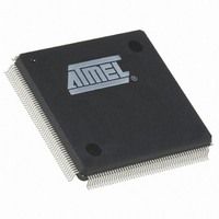
AT40K20-2DQI Atmel, AT40K20-2DQI Datasheet - Page 36

AT40K20-2DQI
Manufacturer Part Number
AT40K20-2DQI
Description
IC FPGA 20K GATES 208PQFP
Manufacturer
Atmel
Series
AT40K/KLVr
Specifications of AT40K20-2DQI
Number Of Logic Elements/cells
1024
Total Ram Bits
8192
Number Of I /o
161
Number Of Gates
30000
Voltage - Supply
4.5 V ~ 5.5 V
Mounting Type
Surface Mount
Operating Temperature
-40°C ~ 85°C
Package / Case
208-BFQFP
Lead Free Status / RoHS Status
Contains lead / RoHS non-compliant
Number Of Labs/clbs
-
Other names
AT40K202DQI
Available stocks
Company
Part Number
Manufacturer
Quantity
Price
AC Timing Characteristics – 3.3V Operation AT40KLV
Delays are based on fixed loads and are described in the notes.
Maximum times based on worst case: V
Minimum times based on best case: V
Notes:
36
Cell Function
Async RAM
Write
Write
Write
Write
Write
Write
Write
Write/Read
Read
Read
Read
Sync RAM
Write
Write
Write
Write
Write
Write
Write
Write
Write
Write/Read
Read
Read
Read
1. CMOS buffer delays are measured from a V
2. Buffer delay is to a pad voltage of 1.5V with one output switching.
3. Parameter based on characterization and simulation; not tested in production.
4. Exact power calculation is available in Atmel FPGA Designer software.
AT40K/AT40KLV Series FPGA
Parameter
t
t
t
t
t
t
t
t
t
t
t
t
t
t
t
t
t
t
t
t
t
t
t
t
WECYC
WEL
WEH
AWS
AWH
DS
DH
DD
AD
OZX
OXZ
CYC
CLKL
CLKH
WCS
WCH
ACS
ACH
DCS
DCH
CD
AD
OZX
OXZ
(Minimum)
(Minimum)
(Maximum)
(Maximum)
(Maximum)
(Maximum)
(Minimum)
(Maximum)
(Maximum)
(Minimum)
(Maximum)
(Maximum)
(Minimum)
(Minimum)
(Minimum)
(Minimum)
(Minimum)
(Minimum)
(Minimum)
(Minimum)
(Minimum)
(Minimum)
(Minimum)
(Minimum)
CC
CC
= 3.6V, temperature = 0°C
= 3.0V, temperature = 70°C
Path
cycle time
we
we
wr addr setup -> we
wr addr hold -> we
din setup -> we
din hold -> we
din -> dout
rd addr -> dout
oe -> dout
oe -> dout
cycle time
clk
clk
we setup -> clk
we hold -> clk
wr addr setup -> clk
wr addr hold -> clk
wr data setup -> clk
wr data hold -> clk
clk -> dout
rd addr -> dout
oe -> dout
oe -> dout
IH
of 1/2 V
CC
at the pad to the internal V
12.0
12.0
5.0
5.0
5.3
0.0
5.0
0.0
8.7
6.3
2.9
3.5
5.0
5.0
3.2
0.0
5.0
0.0
3.9
0.0
5.8
6.3
2.9
3.5
-3
IH
at A. The input buffer load is constant.
Units
ns
ns
ns
ns
ns
ns
ns
ns
ns
ns
ns
ns
ns
ns
ns
ns
ns
ns
ns
ns
ns
ns
ns
ns
Notes
Pulse width low
Pulse width high
rd addr = wr addr
Pulse width low
Pulse width high
rd addr = wr addr
0896C–FPGA–04/02


