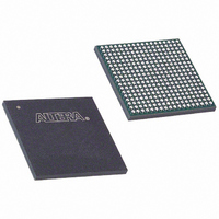
EP1C20F324I7 Altera, EP1C20F324I7 Datasheet - Page 40

EP1C20F324I7
Manufacturer Part Number
EP1C20F324I7
Description
IC CYCLONE FPGA 20K LE 324-FBGA
Manufacturer
Altera
Series
Cyclone®r
Datasheet
1.EP1C3T144C8.pdf
(106 pages)
Specifications of EP1C20F324I7
Number Of Logic Elements/cells
20060
Number Of Labs/clbs
2006
Total Ram Bits
294912
Number Of I /o
233
Voltage - Supply
1.425 V ~ 1.575 V
Mounting Type
Surface Mount
Operating Temperature
-40°C ~ 100°C
Package / Case
324-FBGA
Family Name
Cyclone®
Number Of Logic Blocks/elements
20060
# I/os (max)
233
Frequency (max)
320.1MHz
Process Technology
0.13um (CMOS)
Operating Supply Voltage (typ)
1.5V
Logic Cells
20060
Ram Bits
294912
Operating Supply Voltage (min)
1.425V
Operating Supply Voltage (max)
1.575V
Operating Temp Range
-40C to 100C
Operating Temperature Classification
Industrial
Mounting
Surface Mount
Pin Count
324
Package Type
FBGA
Lead Free Status / RoHS Status
Contains lead / RoHS non-compliant
Number Of Gates
-
Lead Free Status / Rohs Status
Not Compliant
Other names
544-1041
Available stocks
Company
Part Number
Manufacturer
Quantity
Price
Part Number:
EP1C20F324I7
Manufacturer:
ALTERA/阿尔特拉
Quantity:
20 000
Company:
Part Number:
EP1C20F324I7N
Manufacturer:
ALTERA/31
Quantity:
318
Cyclone Device Handbook, Volume 1
Figure 2–26. Cyclone PLL Global Clock Connections
Notes to
(1)
(2)
(3)
(4)
2–34
Preliminary
PLL1_OUT (3), (4)
PLL Counter
Output
Dedicated
Clock Input
Pins
Table 2–7. Global Clock Network Sources (Part 1 of 2)
PLL 1 supports one single-ended or LVDS input via pins CLK0 and CLK1.
PLL2 supports one single-ended or LVDS input via pins CLK2 and CLK3.
PLL1_OUT and PLL2_OUT support single-ended or LVDS output. If external output is not required, these pins are
available as regular user I/O pins.
The EP1C3 device in the 100-pin TQFP package does not support external clock output. The EP1C6 device in the
144-pin TQFP package does not support external clock output from PLL2.
CLK1 (1)
Figure
CLK0
Source
2–26:
PLL1 G0
PLL1 G1
PLL2 G0
PLL2 G1
CLK0
CLK1
CLK2
CLK3
(2)
(2)
(1)
(1)
Figure 2–26
Table 2–7
devices.
PLL1
GCLK0
v
v
—
—
—
—
—
—
g0
g1
e
shows the global clock network sources available in Cyclone
GCLK1
G0
shows the PLL global clock connections.
v
v
—
—
—
—
—
—
G1
G2
G3
GCLK2
v
v
—
—
—
—
—
—
G4
G5
GCLK3
G6
v
v
—
—
—
—
—
—
G7
GCLK4
g0
g1
e
v
v
—
—
—
—
—
—
PLL2
GCLK5
v
v
—
—
—
—
—
—
Altera Corporation
GCLK6
v
v
—
—
—
—
—
—
CLK2
CLK3 (2)
PLL2_OUT (3), (4)
May 2008
GCLK7
v
v
—
—
—
—
—
—


