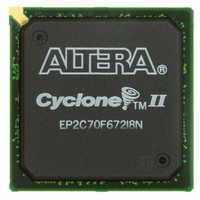
EP2C70F672I8N Altera, EP2C70F672I8N Datasheet - Page 68

EP2C70F672I8N
Manufacturer Part Number
EP2C70F672I8N
Description
IC CYCLONE II FPGA 70K 672-FBGA
Manufacturer
Altera
Series
Cyclone® IIr
Datasheet
1.EP2C5T144C8N.pdf
(168 pages)
Specifications of EP2C70F672I8N
Number Of Logic Elements/cells
68416
Number Of Labs/clbs
4276
Total Ram Bits
1152000
Number Of I /o
422
Voltage - Supply
1.15 V ~ 1.25 V
Mounting Type
Surface Mount
Operating Temperature
-40°C ~ 100°C
Package / Case
672-FBGA
Family Name
Cyclone® II
Number Of Logic Blocks/elements
68416
# I/os (max)
422
Frequency (max)
402.58MHz
Process Technology
90nm
Operating Supply Voltage (typ)
1.2V
Logic Cells
68416
Ram Bits
1152000
Operating Supply Voltage (min)
1.15V
Operating Supply Voltage (max)
1.25V
Operating Temp Range
-40C to 100C
Operating Temperature Classification
Industrial
Mounting
Surface Mount
Pin Count
672
Package Type
FBGA
For Use With
P0304 - DE2-70 CALL FOR ACADEMIC PRICING544-1703 - VIDEO KIT W/CYCLONE II EP2C70N544-1699 - DSP KIT W/CYCLONE II EPS2C70N
Lead Free Status / RoHS Status
Lead free / RoHS Compliant
Number Of Gates
-
Lead Free Status / Rohs Status
Compliant
Other names
544-2143
Available stocks
Company
Part Number
Manufacturer
Quantity
Price
Company:
Part Number:
EP2C70F672I8N
Manufacturer:
ALTERA
Quantity:
490
Part Number:
EP2C70F672I8N
Manufacturer:
BGA
Quantity:
20 000
I/O Structure & Features
2–56
Cyclone II Device Handbook, Volume 1
Cyclone II devices support driver impedance matching to the impedance
of the transmission line, typically 25 or 50 Ω . When used with the output
drivers, on-chip termination sets the output driver impedance to 25 or
50 Ω . Cyclone II devices also support I/O driver series termination
(R
support impedance matching and series termination.
1
On-chip series termination can be supported on any I/O bank. V
V
termination in a given I/O bank. I/O standards that support different R
values can reside in the same I/O bank as long as their V
not conflicting.
1
Impedance matching is implemented using the capabilities of the output
driver and is subject to a certain degree of variation, depending on the
process, voltage and temperature. The actual tolerance is pending silicon
characterization.
Notes to
(1)
(2)
3.3-V LVTTL and LVCMOS
2.5-V LVTTL and LVCMOS
1.8-V LVTTL and LVCMOS
SSTL-2 class I
SSTL-18 class I
Table 2–19. I/O Standards Supporting Series Termination
REF
S
= 50 Ω) for SSTL-2 and SSTL-18.
Supported conditions are V
These R
voltage, and temperature conditions.
must be compatible for all I/O pins in order to enable on-chip series
I/O Standards
Table
The recommended frequency range of operation is pending
silicon characterization.
When using on-chip series termination, programmable drive
strength is not available.
S
values are nominal values. Actual impedance varies across process,
2–19:
CCIO
= V
Target R
CCIO
Table 2–19
25
50
50
50
50
±50 mV.
(2)
(2)
(2)
(2)
(2)
S
(Ω)
lists the I/O standards that
Altera Corporation
CCIO
V
Note (1)
CCIO
February 2007
and V
3.3
2.5
1.8
2.5
1.8
(V)
CCIO
REF
and
are
S


