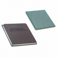
EP2S15F672C3N Altera, EP2S15F672C3N Datasheet - Page 159

EP2S15F672C3N
Manufacturer Part Number
EP2S15F672C3N
Description
IC STRATIX II FPGA 15K 672-FBGA
Manufacturer
Altera
Series
Stratix® IIr
Datasheet
1.EP2S15F484I4N.pdf
(238 pages)
Specifications of EP2S15F672C3N
Number Of Logic Elements/cells
15600
Number Of Labs/clbs
780
Total Ram Bits
419328
Number Of I /o
366
Voltage - Supply
1.15 V ~ 1.25 V
Mounting Type
Surface Mount
Operating Temperature
0°C ~ 85°C
Package / Case
672-FBGA
No. Of Macrocells
15600
Family Type
Stratix II
No. Of I/o's
366
Clock Management
DLL, PLL
I/o Supply Voltage
3.6V
Operating Frequency Max
550MHz
Rohs Compliant
Yes
Lead Free Status / RoHS Status
Lead free / RoHS Compliant
Number Of Gates
-
Other names
544-1880
EP2S15F672C3N
EP2S15F672C3N
Available stocks
Company
Part Number
Manufacturer
Quantity
Price
Company:
Part Number:
EP2S15F672C3N
Manufacturer:
ALTERA
Quantity:
500
- Current page: 159 of 238
- Download datasheet (3Mb)
Altera Corporation
April 2011
4.
5.
The Quartus II software reports the timing with the conditions shown in
Table 5–34
circuit that is represented by the output timing of the Quartus II software.
Figure 5–4. Output Delay Timing Reporting Setup Modeled by Quartus II
Notes to
(1)
(2)
(3)
Figures 5–5
output enable timing.
Record the time to V
Compare the results of steps 2 and 4. The increase or decrease in
delay should be added to or subtracted from the I/O Standard
Output Adder delays to yield the actual worst-case propagation
delay (clock-to-output) of the PCB trace.
Output pin timing is reported at the output pin of the FPGA device. Additional
delays for loading and board trace delay need to be accounted for with IBIS model
simulations.
V
V
CCPD
CCINT
Output
Buffer
Figure
V
GND
CCIO
is 3.085 V unless otherwise specified.
is 1.12 V unless otherwise specified.
using the above equation.
and
5–4:
Output
5–6
V
show the measurement setup for output disable and
MEAS
MEAS
R
.
S
GND
V
TT
R
C
Stratix II Device Handbook, Volume 1
Figure 5–4
T
L
DC & Switching Characteristics
shows the model of the
Output
Output
p
n
R
D
5–23
Related parts for EP2S15F672C3N
Image
Part Number
Description
Manufacturer
Datasheet
Request
R

Part Number:
Description:
CYCLONE II STARTER KIT EP2C20N
Manufacturer:
Altera
Datasheet:

Part Number:
Description:
CPLD, EP610 Family, ECMOS Process, 300 Gates, 16 Macro Cells, 16 Reg., 16 User I/Os, 5V Supply, 35 Speed Grade, 24DIP
Manufacturer:
Altera Corporation
Datasheet:

Part Number:
Description:
CPLD, EP610 Family, ECMOS Process, 300 Gates, 16 Macro Cells, 16 Reg., 16 User I/Os, 5V Supply, 15 Speed Grade, 24DIP
Manufacturer:
Altera Corporation
Datasheet:

Part Number:
Description:
Manufacturer:
Altera Corporation
Datasheet:

Part Number:
Description:
CPLD, EP610 Family, ECMOS Process, 300 Gates, 16 Macro Cells, 16 Reg., 16 User I/Os, 5V Supply, 30 Speed Grade, 24DIP
Manufacturer:
Altera Corporation
Datasheet:

Part Number:
Description:
High-performance, low-power erasable programmable logic devices with 8 macrocells, 10ns
Manufacturer:
Altera Corporation
Datasheet:

Part Number:
Description:
High-performance, low-power erasable programmable logic devices with 8 macrocells, 7ns
Manufacturer:
Altera Corporation
Datasheet:

Part Number:
Description:
Classic EPLD
Manufacturer:
Altera Corporation
Datasheet:

Part Number:
Description:
High-performance, low-power erasable programmable logic devices with 8 macrocells, 10ns
Manufacturer:
Altera Corporation
Datasheet:

Part Number:
Description:
Manufacturer:
Altera Corporation
Datasheet:

Part Number:
Description:
Manufacturer:
Altera Corporation
Datasheet:

Part Number:
Description:
Manufacturer:
Altera Corporation
Datasheet:

Part Number:
Description:
CPLD, EP610 Family, ECMOS Process, 300 Gates, 16 Macro Cells, 16 Reg., 16 User I/Os, 5V Supply, 25 Speed Grade, 24DIP
Manufacturer:
Altera Corporation
Datasheet:


