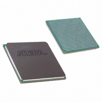
EP2S30F672I4N Altera, EP2S30F672I4N Datasheet - Page 217

EP2S30F672I4N
Manufacturer Part Number
EP2S30F672I4N
Description
IC STRATIX II FPGA 30K 672-FBGA
Manufacturer
Altera
Series
Stratix® IIr
Datasheet
1.EP2S15F484I4N.pdf
(238 pages)
Specifications of EP2S30F672I4N
Number Of Logic Elements/cells
33880
Number Of Labs/clbs
1694
Total Ram Bits
1369728
Number Of I /o
500
Voltage - Supply
1.15 V ~ 1.25 V
Mounting Type
Surface Mount
Operating Temperature
-40°C ~ 100°C
Package / Case
672-FBGA
Lead Free Status / RoHS Status
Lead free / RoHS Compliant
Number Of Gates
-
Other names
544-1900
EP2S30F672I4N
EP2S30F672I4N
Available stocks
Company
Part Number
Manufacturer
Quantity
Price
Company:
Part Number:
EP2S30F672I4N
Manufacturer:
ALTERA
Quantity:
238
- Current page: 217 of 238
- Download datasheet (3Mb)
Altera Corporation
April 2011
Therefore, the DCD percentage for the 267 MHz SSTL-2 Class II
non-DDIO row output clock on a –3 device ranges from 47.5% to 52.5%.
Notes to
(1)
(2)
Column I/O Output
3.3-V LVTTL
3.3-V LVCMOS
2.5 V
1.8 V
1.5-V LVCMOS
SSTL-2 Class I
SSTL-2 Class II
SSTL-18 Class I
SSTL-18 Class II
1.8-V HSTL
Class I
1.8-V HSTL
Class II
1.5-V HSTL
Class I
1.5-V HSTL
Class II
1.2-V HSTL
LVPECL
Table 5–81. Maximum DCD for Non-DDIO Output on Column I/O
Pins
Standard I/O
Standard
The DCD specification is based on a no logic array noise condition.
1.2-V HSTL is only supported in -3 devices.
Table
Note (1)
(2)
5–81:
Maximum DCD for Non-DDIO Output
-3 Devices
190
140
125
185
105
100
170
80
90
70
80
80
85
50
55
Stratix II Device Handbook, Volume 1
DC & Switching Characteristics
-4 & -5 Devices
220
175
155
110
215
135
130
115
100
110
110
115
80
80
-
Unit
ps
ps
ps
ps
ps
ps
ps
ps
ps
ps
ps
ps
ps
ps
ps
5–81
Related parts for EP2S30F672I4N
Image
Part Number
Description
Manufacturer
Datasheet
Request
R

Part Number:
Description:
CYCLONE II STARTER KIT EP2C20N
Manufacturer:
Altera
Datasheet:

Part Number:
Description:
CPLD, EP610 Family, ECMOS Process, 300 Gates, 16 Macro Cells, 16 Reg., 16 User I/Os, 5V Supply, 35 Speed Grade, 24DIP
Manufacturer:
Altera Corporation
Datasheet:

Part Number:
Description:
CPLD, EP610 Family, ECMOS Process, 300 Gates, 16 Macro Cells, 16 Reg., 16 User I/Os, 5V Supply, 15 Speed Grade, 24DIP
Manufacturer:
Altera Corporation
Datasheet:

Part Number:
Description:
Manufacturer:
Altera Corporation
Datasheet:

Part Number:
Description:
CPLD, EP610 Family, ECMOS Process, 300 Gates, 16 Macro Cells, 16 Reg., 16 User I/Os, 5V Supply, 30 Speed Grade, 24DIP
Manufacturer:
Altera Corporation
Datasheet:

Part Number:
Description:
High-performance, low-power erasable programmable logic devices with 8 macrocells, 10ns
Manufacturer:
Altera Corporation
Datasheet:

Part Number:
Description:
High-performance, low-power erasable programmable logic devices with 8 macrocells, 7ns
Manufacturer:
Altera Corporation
Datasheet:

Part Number:
Description:
Classic EPLD
Manufacturer:
Altera Corporation
Datasheet:

Part Number:
Description:
High-performance, low-power erasable programmable logic devices with 8 macrocells, 10ns
Manufacturer:
Altera Corporation
Datasheet:

Part Number:
Description:
Manufacturer:
Altera Corporation
Datasheet:

Part Number:
Description:
Manufacturer:
Altera Corporation
Datasheet:

Part Number:
Description:
Manufacturer:
Altera Corporation
Datasheet:

Part Number:
Description:
CPLD, EP610 Family, ECMOS Process, 300 Gates, 16 Macro Cells, 16 Reg., 16 User I/Os, 5V Supply, 25 Speed Grade, 24DIP
Manufacturer:
Altera Corporation
Datasheet:


