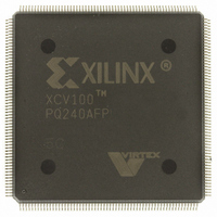
XCV100-5PQ240C Xilinx Inc, XCV100-5PQ240C Datasheet - Page 49

XCV100-5PQ240C
Manufacturer Part Number
XCV100-5PQ240C
Description
IC FPGA 2.5V 108K GATES 240-PQFP
Manufacturer
Xilinx Inc
Series
Virtex™r
Datasheet
1.XCV100-5PQ240C.pdf
(76 pages)
Specifications of XCV100-5PQ240C
Number Of Logic Elements/cells
2700
Number Of Labs/clbs
600
Total Ram Bits
40960
Number Of I /o
166
Number Of Gates
108904
Voltage - Supply
2.375 V ~ 2.625 V
Mounting Type
Surface Mount
Operating Temperature
0°C ~ 85°C
Package / Case
240-BFQFP
Lead Free Status / RoHS Status
Contains lead / RoHS non-compliant
Other names
122-1214
XCV100-5PQ240C
XCV100-5PQ240C
Available stocks
Company
Part Number
Manufacturer
Quantity
Price
DS003-4 (v2.8) July 19, 2002
Virtex Pin Definitions
Table 1: Special Purpose Pins
DS003-4 (v2.8) July 19, 2002
Production Product Specification
GCK0, GCK1,
GCK2, GCK3
M0, M1, M2
CCLK
PROGRAM
DONE
INIT
BUSY/
DOUT
D0/DIN,
D1, D2,
D3, D4,
D5, D6,
D7
WRITE
CS
TDI, TDO,
TMS, TCK
DXN, DXP
V
V
V
GND
CCINT
CCO
REF
© 1999-2002 Xilinx, Inc. All rights reserved. All Xilinx trademarks, registered trademarks, patents, and disclaimers are as listed at http://www.xilinx.com/legal.htm.
Pin Name
All other trademarks and registered trademarks are the property of their respective owners. All specifications are subject to change without notice.
Dedicated
Pin
Yes
Yes
Yes
Yes
Yes
Yes
Yes
Yes
Yes
Yes
No
No
No
No
No
No
R
(Open-drain)
Bidirectional
Bidirectional
Direction
Input or
Input or
Output
Output
Output
Mixed
Input
Input
Input
Input
Input
Input
Input
Input
Input
N/A
0
0
www.xilinx.com
1-800-255-7778
Clock input pins that connect to Global Clock Buffers. These pins become
user inputs when not needed for clocks.
Mode pins are used to specify the configuration mode.
The configuration Clock I/O pin: it is an input for SelectMAP and
slave-serial modes, and output in master-serial mode. After configuration,
it is input only, logic level = Don’t Care.
Initiates a configuration sequence when asserted Low.
Indicates that configuration loading is complete, and that the start-up
sequence is in progress. The output can be open drain.
When Low, indicates that the configuration memory is being cleared. The
pin becomes a user I/O after configuration.
In SelectMAP mode, BUSY controls the rate at which configuration data
is loaded. The pin becomes a user I/O after configuration unless the
SelectMAP port is retained.
In bit-serial modes, DOUT provides header information to downstream
devices in a daisy-chain. The pin becomes a user I/O after configuration.
In SelectMAP mode, D0 - D7 are configuration data pins. These pins
become user I/Os after configuration unless the SelectMAP port is
retained.
In bit-serial modes, DIN is the single data input. This pin becomes a user
I/O after configuration.
In SelectMAP mode, the active-low Write Enable signal. The pin becomes
a user I/O after configuration unless the SelectMAP port is retained.
In SelectMAP mode, the active-low Chip Select signal. The pin becomes
a user I/O after configuration unless the SelectMAP port is retained.
Boundary-scan Test-Access-Port pins, as defined in IEEE 1149.1.
Temperature-sensing diode pins. (Anode: DXP, cathode: DXN)
Power-supply pins for the internal core logic.
Power-supply pins for the output drivers (subject to banking rules)
Input threshold voltage pins. Become user I/Os when an external
threshold voltage is not needed (subject to banking rules).
Ground
0
Virtex™ 2.5 V
Field Programmable Gate Arrays
Production Product Specification
Description
Module 4 of 4
1


