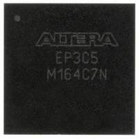
EP3C5M164C7N Altera, EP3C5M164C7N Datasheet - Page 33

EP3C5M164C7N
Manufacturer Part Number
EP3C5M164C7N
Description
IC CYCLONE III FPGA 5K 164 MBGA
Manufacturer
Altera
Series
Cyclone® IIIr
Datasheets
1.EP3C5F256C8N.pdf
(5 pages)
2.EP3C5F256C8N.pdf
(34 pages)
3.EP3C5F256C8N.pdf
(66 pages)
4.EP3C5F256C8N.pdf
(14 pages)
5.EP3C5F256C8N.pdf
(76 pages)
6.EP3C5M164C7N.pdf
(274 pages)
Specifications of EP3C5M164C7N
Number Of Logic Elements/cells
5136
Number Of Labs/clbs
321
Total Ram Bits
423936
Number Of I /o
106
Voltage - Supply
1.15 V ~ 1.25 V
Mounting Type
Surface Mount
Operating Temperature
0°C ~ 85°C
Package / Case
164-MBGA
Family Name
Cyclone III
Number Of Logic Blocks/elements
5136
# I/os (max)
106
Frequency (max)
437.5MHz
Process Technology
65nm
Operating Supply Voltage (typ)
1.2V
Logic Cells
5136
Ram Bits
423936
Operating Supply Voltage (min)
1.15V
Operating Supply Voltage (max)
1.25V
Operating Temp Range
0C to 85C
Operating Temperature Classification
Commercial
Mounting
Surface Mount
Pin Count
164
Package Type
MBGA
For Use With
544-2601 - KIT DEV CYCLONE III LS EP3CLS200544-2411 - KIT DEV NIOS II CYCLONE III ED.
Lead Free Status / RoHS Status
Lead free / RoHS Compliant
Number Of Gates
-
Lead Free Status / Rohs Status
Compliant
Other names
544-2559
Available stocks
Company
Part Number
Manufacturer
Quantity
Price
Company:
Part Number:
EP3C5M164C7N
Manufacturer:
ALTERA
Quantity:
526
Chapter 1: Cyclone III Device Data Sheet
Document Revision History
Table 1–40. Document Revision History
© January 2010 Altera Corporation
May 2008
December 2007
October 2007
July 2007
June 2007
Date
Version
2.0
1.5
1.4
1.3
1.2
(Part 2 of 3)
■
■
■
■
■
■
■
■
■
■
■
■
■
■
■
■
■
■
■
■
■
■
■
■
■
■
■
■
Updated Cyclone III graphic in cover page.
Updated “Operating Conditions” section and included information on
automotive device.
Updated Table 1–3, Table 1–6, and Table 1–7, and added automotive
information.
Under “Pin Capacitance” section, updated Table 1–9 and Table 1–10.
Added new “Schmitt Trigger Input” section with Table 1–12.
Under “I/O Standard Specifications” section, updated Table 1–13, 1–12 and
1–12.
Under “Switching Characteristics” section, updated Table 1–19, 1–15, 1–16,
1–16, 1–17, 1–18, 1–19, 1–20, 1–21, 1–21, 1–23, 1–23, 1–23, 1–24, and
1–25.
Updated Figure 1–5 and 1–29.
Deleted previous Table 1-35 “DDIO Outputs Half-Period Jitter”.
Under “I/O Timing” section, updated Table 1–38, 1–29, 1–32, 1–33, 1–26,
and 1–26.
Under “Typical Design Performance” section updated Table 1–46 through
1–145.
Under “Core Performance Specifications”, updated Tables 1-18 and 1-19.
Under “Preliminary, Correlated, and Final Timing”, updated Table 1-37.
Under “Typical Design Performance”, updated Tables 1-45, 1-46, 1-51, 1-52,
1-57, 1-58, Tables 1-63 through 1-68. 1-69, 1-70, 1-75, 1-76, 1-81, 1-82,
Tables 1-87 through 1-92, Tables 1-99, 1-100, 1-107, and 1-108.
Updated the C
Updated Table 1-21.
Under “High-Speed I/O Specification” section, updated Tables 1-25 through
1-30.
Updated Tables 1-31 through 1-38.
Added new Table 1-32.
Under “Maximum Input and Output Clock Toggle Rate” section, updated
Tables 1-40 through 1-42.
Under “IOE Programmable Delay” section, updated Tables 1-43 through 1-
44.
Under “User I/O Pin Timing Parameters” section, updated Tables 1-45
through 1-92.
Under “Dedicated Clock Pin Timing Parameters” section, updated Tables 1-93
through 1-108.
Updated Table 1-1 with V
Updated R
Added Note (3) to Table 1-12.
Updated t
Updated Table 1-43 and Table 1-44.
Added “Document Revision History” section.
DLOC K
CONF _PD
VREFTB
information in Table 1-19.
information in Tables 1-10.
value in Table 1-9.
ESDHBM
Changes Made
and V
ES DCDM
information.
Cyclone III Device Handbook, Volume 2
1–33


