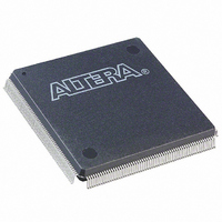
EP1C6Q240C8N Altera, EP1C6Q240C8N Datasheet - Page 37

EP1C6Q240C8N
Manufacturer Part Number
EP1C6Q240C8N
Description
IC CYCLONE FPGA 5980 LE 240-PQFP
Manufacturer
Altera
Series
Cyclone®r
Datasheet
1.EP1C3T144C8.pdf
(106 pages)
Specifications of EP1C6Q240C8N
Number Of Logic Elements/cells
5980
Number Of Labs/clbs
598
Total Ram Bits
92160
Number Of I /o
185
Voltage - Supply
1.425 V ~ 1.575 V
Mounting Type
Surface Mount
Operating Temperature
0°C ~ 85°C
Package / Case
240-MQFP, 240-PQFP
Family Name
Cyclone®
Number Of Logic Blocks/elements
5980
# I/os (max)
185
Frequency (max)
275.03MHz
Process Technology
0.13um (CMOS)
Operating Supply Voltage (typ)
1.5V
Logic Cells
5980
Ram Bits
92160
Operating Supply Voltage (min)
1.425V
Operating Supply Voltage (max)
1.575V
Operating Temp Range
0C to 85C
Operating Temperature Classification
Commercial
Mounting
Surface Mount
Pin Count
240
Package Type
PQFP
Lead Free Status / RoHS Status
Lead free / RoHS Compliant
Number Of Gates
-
Lead Free Status / Rohs Status
Compliant
Other names
544-1813
EP1C6Q240C8N
EP1C6Q240C8N
Available stocks
Company
Part Number
Manufacturer
Quantity
Price
Company:
Part Number:
EP1C6Q240C8N
Manufacturer:
ALTRA
Quantity:
5 510
Company:
Part Number:
EP1C6Q240C8N
Manufacturer:
ALTERA
Quantity:
1 045
Part Number:
EP1C6Q240C8N
Manufacturer:
ALTERA/阿尔特拉
Quantity:
20 000
Figure 2–23. Global Clock Network Multiplexers
Altera Corporation
May 2008
Dual-Purpose Clocks [7..0]
Global Clocks [3..0]
PLL Outputs [3..0]
Core Logic [7..0]
Dual-Purpose Clock Pins
Each Cyclone device except the EP1C3 device has eight dual-purpose
clock pins, DPCLK[7..0] (two on each I/O bank). EP1C3 devices have
five DPCLK pins in the 100-pin TQFP package. These dual-purpose pins
can connect to the global clock network (see
control signals such as clocks, asynchronous clears, presets, and clock
enables, or protocol control signals such as TRDY and IRDY for PCI, or
DQS signals for external memory interfaces.
Combined Resources
Each Cyclone device contains eight distinct dedicated clocking resources.
The device uses multiplexers with these clocks to form six-bit buses to
drive LAB row clocks, column IOE clocks, or row IOE clocks. See
Figure
LAB row clocks to feed the LE registers within the LAB.
IOE clocks have row and column block regions. Six of the eight global
clock resources feed to these row and column regions.
the I/O clock regions.
2–23. Another multiplexer at the LAB level selects two of the six
Global Clock
Network
Clock [7..0]
Global Clock Network and Phase-Locked Loops
Figure
2–22) for high-fanout
Column I/O Region
IO_CLK]5..0]
LAB Row Clock [5..0]
Row I/O Region
IO_CLK[5..0]
Figure 2–24
Preliminary
shows
2–31


