EP3C5E144I7 Altera, EP3C5E144I7 Datasheet - Page 22
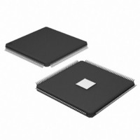
EP3C5E144I7
Manufacturer Part Number
EP3C5E144I7
Description
IC CYCLONE III FPGA 5K 144 EQFP
Manufacturer
Altera
Series
Cyclone® IIIr
Datasheets
1.EP3C5F256C8N.pdf
(5 pages)
2.EP3C5F256C8N.pdf
(34 pages)
3.EP3C5F256C8N.pdf
(66 pages)
4.EP3C5F256C8N.pdf
(14 pages)
5.EP3C5F256C8N.pdf
(76 pages)
Specifications of EP3C5E144I7
Number Of Logic Elements/cells
5136
Number Of Labs/clbs
321
Total Ram Bits
423936
Number Of I /o
94
Voltage - Supply
1.15 V ~ 1.25 V
Mounting Type
Surface Mount
Operating Temperature
-40°C ~ 100°C
Package / Case
144-EQFP
Lead Free Status / RoHS Status
Contains lead / RoHS non-compliant
Number Of Gates
-
Available stocks
Company
Part Number
Manufacturer
Quantity
Price

Company:
Part Number:
EP3C5E144I7N
Manufacturer:
Altera
Quantity:
135
Company:
Part Number:
EP3C5E144I7N
Manufacturer:
ALTERA32
Quantity:
345
Part Number:
EP3C5E144I7N
Manufacturer:
ALTERA/阿尔特拉
Quantity:
20 000


1–12
Table 1–14. Cyclone III Devices Single-Ended SSTL and HSTL I/O Reference Voltage Specifications
Table 1–15. Cyclone III Devices Single-Ended SSTL and HSTL I/O Standards Signal Specifications
Cyclone III Device Handbook, Volume 2
SSTL-2
Class I, II
SSTL-18
Class I, II
HSTL-18
Class I, II
HSTL-15
Class I, II
HSTL-12
Class I, II
Notes to
(1) For an explanation of terms used in
(2) V
(3) Value shown refers to DC input reference voltage, V
(4) Value shown refers to AC input reference voltage, V
Standard
SSTL-2
Class I
SSTL-2
Class II
SSTL-18
Class I
SSTL-18
Class II
HSTL-18
Class I
HSTL-18
Class II
HSTL-15
Class I
HSTL-15
Class II
HSTL-12
Class I
HSTL-12
Class II
Standard
I/O
I/O
TT
of transmitting device must track V
Table
–0.15
–0.15
Min
—
—
—
—
—
—
—
—
f
2.375
1.425
1–14:
1.71
1.14
Min
1.7
V
IL(DC)
(V)
0.125
0.125
V
V
V
V
V
V
V
V
V
V
V
Max
0.18
0.18
0.08
0.08
0.1
0.1
0.1
0.1
CC IO
REF
REF
REF
REF
REF
REF
REF
REF
REF
REF
Typ
For more illustrations of receiver input and transmitter output waveforms, and for
other differential I/O standards, refer to the
Cyclone III Devices
2.5
1.8
1.8
1.5
1.2
–
–
–
–
–
–
–
–
–
–
(V)
2.625
1.575
Max
1.89
1.26
1.9
0.125
0.125
V
V
V
V
V
V
V
V
V
V
0.18
0.18
0.08
0.08
Min
0.1
0.1
0.1
0.1
REF
REF
REF
REF
REF
REF
REF
REF
REF
REF
Table
+
+
+
+
+
+
+
+
+
+
REF
0.48 * V
0.47 * V
V
IH(DC )
1–14, refer to
of the receiving device.
V
V
(V)
0.833
CC IO
CC IO
1.19
0.85
0.71
Min
Max
chapter.
—
—
—
—
—
—
—
—
+ 0.15
+ 0.15
CC IO
CC IO
REF( AC )
REF( DC)
(3)
(4)
“Glossary” on page
.
.
–0.24
–0.24
0.5 * V
0.5 * V
Min
—
—
—
—
—
—
—
—
V
V
IL(AC )
1.25
0.75
REF
Typ
0.9
0.9
C CIO
C CIO
(V)
(V)
V
V
V
V
V
V
V
V
V
V
Max
0.35
0.35
0.25
0.25
0.15
0.15
0.2
0.2
0.2
0.2
(3)
(4)
REF
REF
REF
REF
REF
REF
REF
REF
REF
REF
1–27.
–
–
–
–
–
–
–
–
–
–
0.52 * V
0.53 * V
V
V
V
V
V
V
V
V
V
V
High-Speed Differential Interfaces in
0.35
0.35
0.25
0.25
0.15
0.15
Min
0.2
0.2
0.2
0.2
REF
REF
REF
REF
REF
REF
REF
REF
REF
REF
0.969
+
+
+
+
Max
1.31
0.95
0.79
+
+
+
+
+
+
V
CC IO
CC IO
IH (A C)
V
V
(3)
(4)
(V)
C CIO
C CIO
Max
Chapter 1: Cyclone III Device Data Sheet
—
—
—
—
—
—
—
—
+ 0.24
+ 0.24
V
V
© January 2010 Altera Corporation
REF
REF
0.85
0.71
Min
– 0.04
– 0.04
—
0.25 ×
0.25 ×
V
0.475
V
V
V
Max
0.57
0.76
0.28
V
V
OL
0.4
0.4
0.4
0.4
V
TT
TT
TT
CC IO
CC IO
(Note 1)
(V)
TT
–
–
–
Electrical Characteristics
0.5 * V
(V)
0.75
Typ
V
V
0.9
REF
REF
V
V
(Note 2)
TT
CC IO
0.75 ×
0.75 ×
V
V
V
V
V
0.475
CC IO
V
0.57
V
0.28
Min
V
V
+ 0.76
OH
C CIO
C CIO
0.4
C CIO
0.4
C CIO
0.4
TT
TT
C CIO
C CIO
– 0.4
(V)
+
+
–
–
–
–
V
V
REF
REF
0.95
0.79
Max
+ 0.04
+ 0.04
—
(mA)
16.4
13.4
8.1
6.7
16
16
14
I
8
8
8
OL
–16.4
–13.4
(mA)
–8.1
–6.7
–16
–16
–14
–8
–8
–8
I
OH
Related parts for EP3C5E144I7
Image
Part Number
Description
Manufacturer
Datasheet
Request
R

Part Number:
Description:
CYCLONE II STARTER KIT EP2C20N
Manufacturer:
Altera
Datasheet:


Part Number:
Description:
CPLD, EP610 Family, ECMOS Process, 300 Gates, 16 Macro Cells, 16 Reg., 16 User I/Os, 5V Supply, 35 Speed Grade, 24DIP
Manufacturer:
Altera Corporation
Datasheet:
Part Number:
Description:
CPLD, EP610 Family, ECMOS Process, 300 Gates, 16 Macro Cells, 16 Reg., 16 User I/Os, 5V Supply, 15 Speed Grade, 24DIP
Manufacturer:
Altera Corporation
Datasheet:
Part Number:
Description:
Manufacturer:
Altera Corporation
Datasheet:
Part Number:
Description:
CPLD, EP610 Family, ECMOS Process, 300 Gates, 16 Macro Cells, 16 Reg., 16 User I/Os, 5V Supply, 30 Speed Grade, 24DIP
Manufacturer:
Altera Corporation
Datasheet:
Part Number:
Description:
High-performance, low-power erasable programmable logic devices with 8 macrocells, 10ns
Manufacturer:
Altera Corporation
Datasheet:
Part Number:
Description:
High-performance, low-power erasable programmable logic devices with 8 macrocells, 7ns
Manufacturer:
Altera Corporation
Datasheet:
Part Number:
Description:
Classic EPLD
Manufacturer:
Altera Corporation
Datasheet:
Part Number:
Description:
High-performance, low-power erasable programmable logic devices with 8 macrocells, 10ns
Manufacturer:
Altera Corporation
Datasheet:
Part Number:
Description:
Manufacturer:
Altera Corporation
Datasheet:
Part Number:
Description:
Manufacturer:
Altera Corporation
Datasheet:
Part Number:
Description:
Manufacturer:
Altera Corporation
Datasheet:
Part Number:
Description:
CPLD, EP610 Family, ECMOS Process, 300 Gates, 16 Macro Cells, 16 Reg., 16 User I/Os, 5V Supply, 25 Speed Grade, 24DIP
Manufacturer:
Altera Corporation
Datasheet: