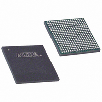
EP1C4F324C8N Altera, EP1C4F324C8N Datasheet - Page 47

EP1C4F324C8N
Manufacturer Part Number
EP1C4F324C8N
Description
IC CYCLONE FPGA 4K LE 324-FBGA
Manufacturer
Altera
Series
Cyclone®r
Datasheet
1.EP1C3T144C8.pdf
(106 pages)
Specifications of EP1C4F324C8N
Number Of Logic Elements/cells
4000
Number Of Labs/clbs
400
Total Ram Bits
78336
Number Of I /o
249
Voltage - Supply
1.425 V ~ 1.575 V
Mounting Type
Surface Mount
Operating Temperature
0°C ~ 85°C
Package / Case
324-FBGA
Family Name
Cyclone®
Number Of Logic Blocks/elements
4000
# I/os (max)
249
Frequency (max)
275.03MHz
Process Technology
0.13um (CMOS)
Operating Supply Voltage (typ)
1.5V
Logic Cells
4000
Ram Bits
78336
Operating Supply Voltage (min)
1.425V
Operating Supply Voltage (max)
1.575V
Operating Temp Range
0C to 85C
Operating Temperature Classification
Commercial
Mounting
Surface Mount
Pin Count
324
Package Type
FBGA
Lead Free Status / RoHS Status
Lead free / RoHS Compliant
Number Of Gates
-
Lead Free Status / Rohs Status
Compliant
Other names
544-1804
EP1C4F324C8N
EP1C4F324C8N
Available stocks
Company
Part Number
Manufacturer
Quantity
Price
Company:
Part Number:
EP1C4F324C8N
Manufacturer:
ALTERA
Quantity:
648
Part Number:
EP1C4F324C8N
Manufacturer:
ALTERA
Quantity:
20 000
Figure 2–28. Row I/O Block Connection to the Interconnect
Notes to
(1)
(2)
Altera Corporation
May 2008
The 21 data and control signals consist of three data out lines, io_dataout[2..0], three output enables,
io_coe[2..0], three input clock enables, io_cce_in[2..0], three output clock enables, io_cce_out[2..0],
three clocks, io_cclk[2..0], three asynchronous clear signals, io_caclr[2..0], and three synchronous clear
signals, io_csclr[2..0].
Each of the three IOEs in the row I/O block can have one io_datain input (combinatorial or registered) and one
comb_io_datain (combinatorial) input.
LAB Local
Interconnect
Figure
R4 Interconnects
to Adjacent LAB
Interconnect
Direct Link
2–28:
LAB
io_datain[2..0] and
comb_io_datain[2..0] (2)
C4 Interconnects
from Adjacent LAB
Interconnect
Direct Link
I/O Block Local
Interconnect
io_clk[5:0]
21
I/O Block
Row I/O Block
Contains up to
Row
Three IOEs
21 Data and
Control Signals
from Logic Array (1)
I/O Structure
Preliminary
2–41


