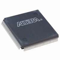
EPF10K10QC208-4 Altera, EPF10K10QC208-4 Datasheet - Page 38

EPF10K10QC208-4
Manufacturer Part Number
EPF10K10QC208-4
Description
IC FLEX 10K FPGA 10K 208-PQFP
Manufacturer
Altera
Series
FLEX-10K®r
Datasheet
1.EPF10K10ATC100-3.pdf
(128 pages)
Specifications of EPF10K10QC208-4
Number Of Logic Elements/cells
576
Number Of Labs/clbs
72
Total Ram Bits
6144
Number Of I /o
134
Number Of Gates
31000
Voltage - Supply
4.75 V ~ 5.25 V
Mounting Type
Surface Mount
Operating Temperature
0°C ~ 85°C
Package / Case
208-MQFP, 208-PQFP
Family Name
FLEX 10K
Number Of Usable Gates
10000
Number Of Logic Blocks/elements
576
# Registers
450
# I/os (max)
134
Frequency (max)
125MHz
Process Technology
CMOS
Operating Supply Voltage (typ)
5V
Logic Cells
576
Ram Bits
6144
Device System Gates
31000
Operating Supply Voltage (min)
4.75V
Operating Supply Voltage (max)
5.25V
Operating Temp Range
0C to 70C
Operating Temperature Classification
Commercial
Mounting
Surface Mount
Pin Count
208
Package Type
PQFP
Lead Free Status / RoHS Status
Contains lead / RoHS non-compliant
Other names
544-2196
Available stocks
Company
Part Number
Manufacturer
Quantity
Price
Company:
Part Number:
EPF10K10QC208-4
Manufacturer:
ALTERA
Quantity:
10
Company:
Part Number:
EPF10K10QC208-4
Manufacturer:
ALTERA
Quantity:
586
Part Number:
EPF10K10QC208-4
Manufacturer:
ALTERA
Quantity:
20 000
Company:
Part Number:
EPF10K10QC208-4*
Manufacturer:
RCA
Quantity:
3
Company:
Part Number:
EPF10K10QC208-4N
Manufacturer:
ALTERA20
Quantity:
144
Output
Configuration
38
FLEX 10K Embedded Programmable Logic Device Family Data Sheet
Figure 17. Enabling ClockLock & ClockBoost in the Same Design
To use both the ClockLock and ClockBoost circuits in the same design,
designers must use Revision C EPF10K100GC503-3DX devices and
MAX+PLUS II software versions 7.2 or higher. The die revision is
indicated by the third digit of the nine-digit code on the top side of the
device.
This section discusses the peripheral component interconnect (PCI)
pull-up clamping diode option, slew-rate control, open-drain output
option, MultiVolt I/O interface, and power sequencing for FLEX 10K
devices. The PCI pull-up clamping diode, slew-rate control, and
open-drain output options are controlled pin-by-pin via Altera logic
options. The MultiVolt I/O interface is controlled by connecting V
a different voltage than V
software via the Global Project Device Options dialog box (Assign
menu).
PCI Clamping Diodes
The EPF10K10A and EPF10K30A devices have a pull-up clamping diode
on every I/O, dedicated input, and dedicated clock pin. PCI clamping
diodes clamp the transient overshoot caused by reflected waves to the
V
can also be used to limit overshoot in other systems.
Clamping diodes are controlled on a pin-by-pin basis via a logic option in
the Altera software. When V
diode turned on can be driven by a 2.5-V or 3.3-V signal, but not a 5.0-V
signal. When V
can be driven by a 2.5-V signal, but not a 3.3-V or 5.0-V signal. However,
a clamping diode can be turned on for a subset of pins, which allows
devices to bridge between a 3.3-V PCI bus and a 5.0-V device.
CCIO
value and are required for 3.3-V PCI compliance. Clamping diodes
gclk1
CCIO
CLKLOCK
CLKLOCK
is 2.5 V, a pin that has the clamping diode turned on
CCINT
CLOCKBOOST=1
INPUT_FREQUENCY=50
CLOCKBOOST=2
INPUT_FREQUENCY=50
CCIO
. Its effect can be simulated in the Altera
a
b
is 3.3 V, a pin that has the clamping
D
D
Q
Q
Altera Corporation
aout
bout
CCIO
to


