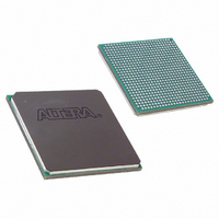
EP2S30F672C5 Altera, EP2S30F672C5 Datasheet - Page 142

EP2S30F672C5
Manufacturer Part Number
EP2S30F672C5
Description
IC STRATIX II FPGA 30K 672-FBGA
Manufacturer
Altera
Series
Stratix® IIr
Datasheet
1.EP2S15F484I4N.pdf
(238 pages)
Specifications of EP2S30F672C5
Number Of Logic Elements/cells
33880
Number Of Labs/clbs
1694
Total Ram Bits
1369728
Number Of I /o
500
Voltage - Supply
1.15 V ~ 1.25 V
Mounting Type
Surface Mount
Operating Temperature
0°C ~ 85°C
Package / Case
672-FBGA
Family Name
Stratix II
Number Of Logic Blocks/elements
33880
# I/os (max)
500
Frequency (max)
609.76MHz
Process Technology
90nm (CMOS)
Operating Supply Voltage (typ)
1.2V
Logic Cells
33880
Ram Bits
1369728
Operating Supply Voltage (min)
1.15V
Operating Supply Voltage (max)
1.25V
Operating Temp Range
0C to 85C
Operating Temperature Classification
Commercial
Mounting
Surface Mount
Pin Count
672
Package Type
FBGA
Lead Free Status / RoHS Status
Contains lead / RoHS non-compliant
Number Of Gates
-
Lead Free Status / Rohs Status
Not Compliant
Other names
544-1126
Available stocks
Company
Part Number
Manufacturer
Quantity
Price
Company:
Part Number:
EP2S30F672C5K
Manufacturer:
ALTERA
Quantity:
220
Company:
Part Number:
EP2S30F672C5N
Manufacturer:
ALTERA
Quantity:
238
Part Number:
EP2S30F672C5N
Manufacturer:
ALTERA/阿尔特拉
Quantity:
20 000
Operating Conditions
5–6
Stratix II Device Handbook, Volume 1
Notes to
(1)
(2)
Notes to
(1)
(2)
V
V
V
V
V
V
V
V
V
V
Table 5–8. 1.8-V I/O Specifications
Table 5–9. 1.5-V I/O Specifications
CCIO
I H
IL
OH
OL
CCIO
I H
IL
OH
OL
Symbol
Symbol
The Stratix II device family’s V
Range of the EIA/JEDEC standard.
This specification is supported across all the programmable drive settings available for this I/O standard as shown
in the Stratix II Architecture chapter in volume 1 of the Stratix II Device Handbook.
The Stratix II device family’s V
Range of the EIA/JEDEC standard.
This specification is supported across all the programmable drive settings available for this I/O standard as shown
in the Stratix II Architecture chapter in volume 1 of the Stratix II Device Handbook.
(1)
(1)
Table
Table
Output supply voltage
High-level input voltage
Low-level input voltage
High-level output voltage
Low-level output voltage
Output supply voltage
High-level input voltage
Low-level input voltage
High-level output voltage
Low-level output voltage
5–8:
5–9:
Parameter
Parameter
Figures 5–1
waveforms, respectively, for all differential I/O standards (LVDS,
LVPECL, and HyperTransport technology).
C C I O
C C I O
voltage level support of 1.8 ± -5% is narrower than defined in the Normal
voltage level support of 1.5 ± -5% is narrower than defined in the Normal
and
I
I
I
I
OH
OL
OH
OL
5–2
= 2 mA
= 2 mA
= –2 mA
= –2 mA
show receiver input and transmitter output
Conditions
Conditions
(2)
(2)
(2)
(2)
0.65 × V
V
0.65 × V
0.75 × V
Minimum
Minimum
CCIO
–0.30
1.425
–0.30
1.71
– 0.45
CCIO
CCIO
CCIO
0.35 × V
V
0.35 × V
0.25 × V
Altera Corporation
Maximum
Maximum
CCIO
1.575
1.89
2.25
0.45
+ 0.30
CCIO
CCIO
CCIO
April 2011
Unit
Unit
V
V
V
V
V
V
V
V
V
V


