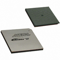
EP2SGX130GF1508I4 Altera, EP2SGX130GF1508I4 Datasheet - Page 211

EP2SGX130GF1508I4
Manufacturer Part Number
EP2SGX130GF1508I4
Description
IC STRATIX II GX 130K 1508-FBGA
Manufacturer
Altera
Series
Stratix® II GXr
Datasheet
1.EP2SGX30DF780C5.pdf
(316 pages)
Specifications of EP2SGX130GF1508I4
Number Of Logic Elements/cells
132540
Number Of Labs/clbs
6627
Total Ram Bits
6747840
Number Of I /o
734
Voltage - Supply
1.15 V ~ 1.25 V
Mounting Type
Surface Mount
Operating Temperature
-40°C ~ 100°C
Package / Case
1508-FBGA
Family Name
Stratix II GX
Number Of Logic Blocks/elements
132540
# I/os (max)
734
Frequency (max)
732.1MHz
Process Technology
SRAM
Operating Supply Voltage (typ)
1.2V
Logic Cells
132540
Ram Bits
6747840
Operating Supply Voltage (min)
1.15V
Operating Supply Voltage (max)
1.25V
Operating Temp Range
-40C to 100C
Operating Temperature Classification
Industrial
Mounting
Surface Mount
Pin Count
1508
Package Type
FC-FBGA
Lead Free Status / RoHS Status
Contains lead / RoHS non-compliant
Number Of Gates
-
Lead Free Status / Rohs Status
Not Compliant
Other names
544-2174
Available stocks
Company
Part Number
Manufacturer
Quantity
Price
Company:
Part Number:
EP2SGX130GF1508I4N
Manufacturer:
Sunon
Quantity:
1 000
Part Number:
EP2SGX130GF1508I4N
Manufacturer:
ALTERA/阿尔特拉
Quantity:
20 000
- Current page: 211 of 316
- Download datasheet (2Mb)
Altera Corporation
June 2009
Notes to
(1)
(2)
(3)
(4)
Functional
BASIC
Double
Width
Table 4–22. PCS Latency (Part 3 of 3)
Mode
The latency numbers are with respect to the PLD-transceiver interface clock cycles.
The total latency number is rounded off in the Sum column.
The rate matcher latency shown is the steady state latency. Actual latency may vary depending on the skip ordered set
gap allowed by the protocol, actual PPM difference between the reference clocks, and so forth.
For CPRI 614 Mbps and 1.228 Gbps data rates, the Quartus II software customizes the PLD-transceiver interface clocking
to achieve zero clock cycle uncertainty in the receiver phase compensation FIFO latency. For more details, refer to the CPRI
Mode section in the
Table
Configuration
width; with
width; with
16/20-bit
16/20-bit
32/40-bit
32/40-bit
Matcher
Matcher
Matcher
Matcher
channel
channel
channel
channel
without
without
width;
width;
Rate
Rate
Rate
Rate
4–21:
Stratix II GX Transceiver Architecture Overview
Aligner
2-2.5
2-2.5
Word
4-5
4-5
Deskew
FIFO
-
-
-
-
Note (1)
5.5-6.5
Matcher
11-13
Rate
(3)
-
-
Decoder
8B/10B
0.5
0.5
1
1
Receiver PCS Latency
Receiver
Machine
State
-
-
-
-
chapter in volume 2 of the Stratix II GX Device Handbook
Stratix II GX Device Handbook, Volume 1
serializer
Byte
De-
1
1
1
1
DC and Switching Characteristics
Order
Byte
1-3
1
1
1
Receiver
Phase
Comp
FIFO
1-2
1-2
1-2
1-2
Receiver
PIPE
-
-
-
-
4–41
19-23
11-14
8-10
Sum
6-9
(2)
Related parts for EP2SGX130GF1508I4
Image
Part Number
Description
Manufacturer
Datasheet
Request
R

Part Number:
Description:
CYCLONE II STARTER KIT EP2C20N
Manufacturer:
Altera
Datasheet:

Part Number:
Description:
CPLD, EP610 Family, ECMOS Process, 300 Gates, 16 Macro Cells, 16 Reg., 16 User I/Os, 5V Supply, 35 Speed Grade, 24DIP
Manufacturer:
Altera Corporation
Datasheet:

Part Number:
Description:
CPLD, EP610 Family, ECMOS Process, 300 Gates, 16 Macro Cells, 16 Reg., 16 User I/Os, 5V Supply, 15 Speed Grade, 24DIP
Manufacturer:
Altera Corporation
Datasheet:

Part Number:
Description:
Manufacturer:
Altera Corporation
Datasheet:

Part Number:
Description:
CPLD, EP610 Family, ECMOS Process, 300 Gates, 16 Macro Cells, 16 Reg., 16 User I/Os, 5V Supply, 30 Speed Grade, 24DIP
Manufacturer:
Altera Corporation
Datasheet:

Part Number:
Description:
High-performance, low-power erasable programmable logic devices with 8 macrocells, 10ns
Manufacturer:
Altera Corporation
Datasheet:

Part Number:
Description:
High-performance, low-power erasable programmable logic devices with 8 macrocells, 7ns
Manufacturer:
Altera Corporation
Datasheet:

Part Number:
Description:
Classic EPLD
Manufacturer:
Altera Corporation
Datasheet:

Part Number:
Description:
High-performance, low-power erasable programmable logic devices with 8 macrocells, 10ns
Manufacturer:
Altera Corporation
Datasheet:

Part Number:
Description:
Manufacturer:
Altera Corporation
Datasheet:

Part Number:
Description:
Manufacturer:
Altera Corporation
Datasheet:

Part Number:
Description:
Manufacturer:
Altera Corporation
Datasheet:

Part Number:
Description:
CPLD, EP610 Family, ECMOS Process, 300 Gates, 16 Macro Cells, 16 Reg., 16 User I/Os, 5V Supply, 25 Speed Grade, 24DIP
Manufacturer:
Altera Corporation
Datasheet:


