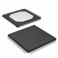
XC3S100E-4TQG144I Xilinx Inc, XC3S100E-4TQG144I Datasheet - Page 33

XC3S100E-4TQG144I
Manufacturer Part Number
XC3S100E-4TQG144I
Description
IC FPGA SPARTAN-3E 100K 144-TQFP
Manufacturer
Xilinx Inc
Series
Spartan™-3Er
Datasheet
1.XC3S100E-4TQG144I.pdf
(193 pages)
Specifications of XC3S100E-4TQG144I
Package / Case
144-TQFP, 144-VQFP
Mounting Type
Surface Mount
Voltage - Supply
1.1 V ~ 3.465 V
Operating Temperature
-40°C ~ 100°C
Number Of I /o
108
Number Of Logic Elements/cells
*
Number Of Gates
*
Lead Free Status / RoHS Status
Lead free / RoHS Compliant
Available stocks
Company
Part Number
Manufacturer
Quantity
Price
Company:
Part Number:
XC3S100E-4TQG144I
Manufacturer:
XILINX/21
Quantity:
163
Company:
Part Number:
XC3S100E-4TQG144I
Manufacturer:
Xilinx Inc
Quantity:
10 000
Part Number:
XC3S100E-4TQG144I
Manufacturer:
XILINX/赛灵思
Quantity:
20 000
- Current page: 33 of 193
- Download datasheet (2Mb)
Functional Description
Each shift register provides a shift output MC15 for the last
bit in each LUT, in addition to providing addressable access
to any bit in the shift register through the normal D output.
The address inputs A[3:0] are the same as the distributed
RAM address lines, which come from the LUT inputs F[4:1]
or G[4:1]. At the end of the shift register, the CLB flip-flop
can be used to provide one more shift delay for the addres-
sable bit.
The shift register element is known as the SRL16 (Shift
Register LUT 16-bit), with a ‘C’ added to signify a cascade
ability (Q15 output) and ‘E’ to indicate a Clock Enable. See
Figure 26
26
CE (SR)
DI (BY)
A[3:0]
SHIFTIN
CLK
Figure 25: Logic Cell SRL16 Structure
for an example of the SRLC16E component.
4
WE
CK
A[3:0]
WS
SRLC16
WSG
SHIFT-REG
MC15
DI
D
SHIFTOUT
or YB
(optional)
D
Q
X465_03_040203
Output
Registered
Output
www.xilinx.com
I
The functionality of the shift register is shown in
The SRL16 shifts on the rising edge of the clock input when
the Clock Enable control is High. This shift register cannot
be initialized either during configuration or during operation
except by shifting data into it. The clock enable and clock
inputs are shared between the two LUTs in a SLICEM. The
clock enable input is automatically kept active if unused.
Table 17: SRL16 Shift Register Function
For more information on the SRL16, refer to XAPP465:
"Using Look-Up Tables as Shift Registers (SRL16) in
Spartan-3 FPGAs".
Notes:
1.
Am
Am
Am
Figure 26: SRL16 Shift Register Component with
m = 0, 1, 2, 3.
CLK
X
↑
Inputs
Cascade and Clock Enable
CE
0
1
CLK
CE
A0
A1
A2
A3
D
SRLC16E
D
D
X
Advance Product Specification
DS312-2 (v1.1) March 21, 2005
DS312-2_43_021305
Q[Am-1]
Q[Am]
Q
Q15
Q
Outputs
Q[15]
Q[15]
Q15
Table
17.
R
Related parts for XC3S100E-4TQG144I
Image
Part Number
Description
Manufacturer
Datasheet
Request
R

Part Number:
Description:
IC SPARTAN-3E FPGA 100K 144-TQFP
Manufacturer:
Xilinx Inc
Datasheet:

Part Number:
Description:
FIELD PROGRAMMER
Manufacturer:
Xilinx Inc
Datasheet:

Part Number:
Description:
FPGA Spartan®-3E Family 100K Gates 2160 Cells 572MHz 90nm (CMOS) Technology 1.2V 100-Pin VTQFP
Manufacturer:
Xilinx Inc
Datasheet:

Part Number:
Description:
FPGA Spartan®-3E Family 100K Gates 2160 Cells 572MHz 90nm (CMOS) Technology 1.2V 144-Pin TQFP
Manufacturer:
Xilinx Inc
Datasheet:

Part Number:
Description:
FPGA Spartan®-3E Family 100K Gates 2160 Cells 657MHz 90nm (CMOS) Technology 1.2V 144-Pin TQFP
Manufacturer:
Xilinx Inc
Datasheet:

Part Number:
Description:
Spartan-3E FPGA Family
Manufacturer:
XILINX [Xilinx, Inc]
Datasheet:

Part Number:
Description:
Spartan-3E FPGA Family: Complete Data Sheet
Manufacturer:
XILINX [Xilinx, Inc]
Datasheet:

Part Number:
Description:
IC FPGA SPARTAN-3E 100K 100-VQFP
Manufacturer:
Xilinx Inc
Datasheet:

Part Number:
Description:
IC FPGA SPARTAN-3E 100K 132CSBGA
Manufacturer:
Xilinx Inc
Datasheet:

Part Number:
Description:
IC FPGA SPARTAN-3E 100K 132CSBGA
Manufacturer:
Xilinx Inc
Datasheet:

Part Number:
Description:
IC FPGA SPARTAN-3E 100K 144-TQFP
Manufacturer:
Xilinx Inc
Datasheet:

Part Number:
Description:
IC FPGA SPARTAN 3E 100VQFP
Manufacturer:
Xilinx Inc
Datasheet:

Part Number:
Description:
IC FPGA SPARTAN 3E 144TQFP
Manufacturer:
Xilinx Inc
Datasheet:

Part Number:
Description:
FPGA Spartan®-3E Family 100K Gates 2160 Cells 572MHz 90nm (CMOS) Technology 1.2V 132-Pin CSBGA
Manufacturer:
Xilinx Inc
Datasheet:

Part Number:
Description:
IC CPLD .8K 36MCELL 44-VQFP
Manufacturer:
Xilinx Inc
Datasheet:


