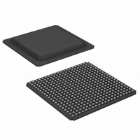
XC3S400AN-4FGG400C Xilinx Inc, XC3S400AN-4FGG400C Datasheet - Page 63

XC3S400AN-4FGG400C
Manufacturer Part Number
XC3S400AN-4FGG400C
Description
IC SPARTAN-3AN FPGA 400K 400FBGA
Manufacturer
Xilinx Inc
Series
Spartan™-3ANr
Datasheets
1.XC3S50A-4VQG100C.pdf
(7 pages)
2.XC3S50AN-4TQG144C.pdf
(2 pages)
3.XC3S50AN-4TQG144C.pdf
(123 pages)
Specifications of XC3S400AN-4FGG400C
Total Ram Bits
368640
Number Of Logic Elements/cells
8064
Number Of Labs/clbs
896
Number Of I /o
311
Number Of Gates
400000
Voltage - Supply
1.14 V ~ 1.26 V
Mounting Type
Surface Mount
Operating Temperature
0°C ~ 85°C
Package / Case
400-BGA
No. Of Logic Blocks
8064
No. Of Gates
400000
No. Of Macrocells
8064
Family Type
Spartan-3AN
No. Of Speed Grades
4
No. Of I/o's
311
Lead Free Status / RoHS Status
Lead free / RoHS Compliant
Other names
122-1554
Available stocks
Company
Part Number
Manufacturer
Quantity
Price
Company:
Part Number:
XC3S400AN-4FGG400C
Manufacturer:
XILINX
Quantity:
3 340
Company:
Part Number:
XC3S400AN-4FGG400C
Manufacturer:
Xilinx Inc
Quantity:
10 000
Part Number:
XC3S400AN-4FGG400C
Manufacturer:
XILINX
Quantity:
20 000
Table 54: Slave Mode CCLK Input Low and High Time
Master Serial and Slave Serial Mode Timing
X-Ref Target - Figure 14
Table 55: Timing for the Master Serial and Slave Serial Configuration Modes
DS557 (v4.1) April 1, 2011
Product Specification
Notes:
1.
2.
(Input/Output)
T
T
Clock-to-Output Times
T
Setup Times
T
Hold Times
T
Clock Timing
T
T
F
(Open-Drain)
SCCL,
SCCH
CCO
DCC
CCD
CCH
CCL
CCSER
Symbol
Symbol
PROG_B
The numbers in this table are based on the operating conditions set forth in
For serial configuration with a daisy-chain of multiple FPGAs, the maximum limit is 25 MHz.
(Output)
INIT_B
(Input)
(Input)
CCLK
DOUT
DIN
CCLK Low and High time
The time from the falling transition on the CCLK pin to data appearing at the
DOUT pin
The time from the setup of data at the DIN pin to the rising transition at the
CCLK pin
The time from the rising transition at the CCLK pin to the point when data is
last held at the DIN pin
High pulse width at the CCLK input pin
Low pulse width at the CCLK input pin
Frequency of the clock signal at the
CCLK input pin
Figure 14: Waveforms for Master Serial and Slave Serial Configuration
(2)
Description
T
DCC
Description
Bit 0
No bitstream compression
With bitstream compression
www.xilinx.com
T
Spartan-3AN FPGA Family: DC and Switching Characteristics
CCD
Bit 1
Table
10.
T
T
Master
Master
Master
Master
Slave/
MCCL
SCCL
Slave
Slave
Slave
Slave
Both
Both
Bit n
1/F
CCSER
T
Min
CCO
5
Bit n-64
Bit n+1
All Speed Grades
Min
1.5
1.0
T
7
0
0
0
T
SCCH
MCCH
See
See
See
See
Max
Bit n-63
Table 53
Table 54
Table 53
Table 54
Max
100
100
10
–
–
DS312-3_05_103105
Units
ns
Units
MHz
MHz
ns
ns
ns
63


