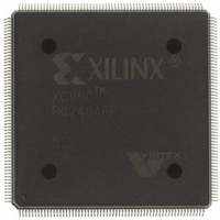
XCV50-5PQ240C Xilinx Inc, XCV50-5PQ240C Datasheet - Page 37

XCV50-5PQ240C
Manufacturer Part Number
XCV50-5PQ240C
Description
IC FPGA 2.5V 57K GATES 240-PQFP
Manufacturer
Xilinx Inc
Series
Virtex™r
Datasheet
1.XCV100-5PQ240C.pdf
(76 pages)
Specifications of XCV50-5PQ240C
Number Of Logic Elements/cells
1728
Number Of Labs/clbs
384
Total Ram Bits
32768
Number Of I /o
166
Number Of Gates
57906
Voltage - Supply
2.375 V ~ 2.625 V
Mounting Type
Surface Mount
Operating Temperature
0°C ~ 85°C
Package / Case
240-BFQFP
Lead Free Status / RoHS Status
Contains lead / RoHS non-compliant
Other names
122-1213
XCV50-5PQ240C
XCV50-5PQ240C
Available stocks
Company
Part Number
Manufacturer
Quantity
Price
Company:
Part Number:
XCV50-5PQ240C
Manufacturer:
XILINX
Quantity:
1 238
Company:
Part Number:
XCV50-5PQ240C
Manufacturer:
XilinxInc
Quantity:
3 000
CLB Switching Characteristics
Delays originating at F/G inputs vary slightly according to the input used. The values listed below are worst-case. Precise
values are provided by the timing analyzer.
DS003-3 (v3.2) September 10, 2002
Production Product Specification
Notes:
1.
Combinatorial Delays
4-input function: F/G inputs to X/Y outputs
5-input function: F/G inputs to F5 output
5-input function: F/G inputs to X output
6-input function: F/G inputs to Y output via F6 MUX
6-input function: F5IN input to Y output
Incremental delay routing through transparent latch
to XQ/YQ outputs
BY input to YB output
Sequential Delays
FF Clock CLK to XQ/YQ outputs
Latch Clock CLK to XQ/YQ outputs
Setup and Hold Times before/after Clock CLK
4-input function: F/G Inputs
5-input function: F/G inputs
6-input function: F5IN input
6-input function: F/G inputs via F6 MUX
BX/BY inputs
CE input
SR/BY inputs (synchronous)
Clock CLK
Minimum Pulse Width, High
Minimum Pulse Width, Low
Set/Reset
Minimum Pulse Width, SR/BY inputs
Delay from SR/BY inputs to XQ/YQ outputs
(asynchronous)
Delay from GSR to XQ/YQ outputs
Toggle Frequency (MHz) (for export control)
A Zero "0" Hold Time listing indicates no hold time or a negative hold time. Negative values cannot be guaranteed "best-case", but
if a "0" is listed, there is no positive hold time.
R
Description
(1)
www.xilinx.com
1-800-255-7778
T
T
F5INCK
T
T
T
F
IF5CK
IF6CK
CECK
T
T
DICK
TOG
T
T
RCK
Symbol
T
ICK
T
T
IOGSRQ
T
T
T
T
IFNCTL
T
T
T
T
F5INY
T
BYYB
CKLO
RPW
IF5X
IF6Y
CKO
ILO
IF5
CH
RQ
CL
/T
/T
/T
/T
/T
/T
(MHz)
T
CKR
CKI
CKIF5
CKF5IN
CKIF6
CKDI
CKCE
Virtex™ 2.5 V Field Programmable Gate Arrays
0.46 / 0
0.30 / 0
0.37 / 0
0.33 / 0
0.6 / 0
0.7 / 0
0.8 / 0
Setup Time / Hold Time
0.29
0.32
0.36
0.44
0.17
0.31
0.27
0.54
0.54
Min
625
0.6
0.8
0.8
1.3
4.9
1.2 / 0
1.3 / 0
1.0 / 0
1.5 / 0
0.6 / 0
0.8 / 0
0.7 / 0
Speed Grade
0.32
0.53
333
0.6
0.7
0.8
0.9
0.7
1.1
1.2
1.5
1.5
2.5
1.1
9.7
-6
1.4 / 0
1.5 / 0
1.1 / 0
1.7 / 0
0.7 / 0
0.9 / 0
0.8 / 0
0.36
10.9
294
0.7
0.8
0.8
1.0
0.7
0.6
1.2
1.4
1.7
1.7
2.8
1.3
-5
1.5 / 0
1.7 / 0
1.2 / 0
1.9 / 0
0.8 / 0
1.0 / 0
0.9 / 0
0.42
12.5
250
0.8
0.9
1.0
1.2
0.8
0.7
1.4
1.6
2.0
2.0
3.3
1.4
-4
Module 3 of 4
ns, max
ns, max
ns, max
ns, max
ns, max
ns, max
ns, max
ns, max
ns, max
ns, max
ns, max
ns, min
ns, min
ns, min
ns, min
ns, min
ns, min
ns, min
ns, min
ns, min
ns, min
Units
MHz
13


